MC100LVEL37DW ON Semiconductor, MC100LVEL37DW Datasheet
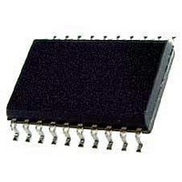
Clock Drivers & Distribution 3.3V ECL Clock

MC100LVEL37DW

Manufacturer Part Number
MC100LVEL37DW
Description
Clock Drivers & Distribution 3.3V ECL Clock
Manufacturer
ON Semiconductor
Type
ECLr
Datasheet

Specifications of MC100LVEL37DW

Minimum Operating Temperature
- 40 C
Mounting Style
SMD/SMT
Multiply / Divide Factor
2:1
Number Of Clock Inputs
2
Output Logic Level
ECL
Supply Voltage (max)
+/- 3.8 V
Supply Voltage (min)
+/- 3 V
Maximum Operating Temperature
+ 85 C
Package / Case
SOIC-20 Wide
Lead Free Status / RoHS Status
Lead free / RoHS Compliant

Available stocks

Company
Part Number
Manufacturer
Quantity
Price
Part Number:
MC100LVEL37DWR
Manufacturer:
ON/安森美
Quantity:
20 000
Part Number:
MC100LVEL37DWR2G
Manufacturer:
ON/安森美
Quantity:
20 000
Part Number:
MC100LVEL37DWR2G
Manufacturer:
ON
Quantity:
13 836
MC100LVEL37
3.3V ECL 1:4 ÷1/÷2 Clock
Fanout Buffer
Description
device offers two outputs at ÷1 of the input frequency, and two outputs
at ÷2 of the input frequency. The Low Output−Output Skew of the
device makes it ideal for distributing 1x and 1/2x frequency
synchronous signals.
stability under open input conditions. When both differential inputs
are left open the CLKn input will pull down to V
will bias around V
Features
*For additional information on our Pb−Free strategy and soldering details, please
© Semiconductor Components Industries, LLC, 2008
November, 2008 − Rev. 6
download the ON Semiconductor Soldering and Mounting Techniques
Reference Manual, SOLDERRM/D.
The MC100LVEL37 is a fully differential 1:4 fanout buffer. The
The differential inputs have special circuitry which ensures device
>200 V Machine Model
with V
with V
For Additional Information, see Application Note AND8003/D
Oxygen Index 28 to 34
700 ps Typical Propagation Delays
50 ps Maximum Output−Output Skews
ESD Protection: >2 kV Human Body Model,
The 100 Series Contains Temperature Compensation
PECL Mode Operating Range: V
NECL Mode Operating Range: V
Internal Input Pulldown Resistors
Qn Output will Default LOW with Inputs Open or at V
Meets or Exceeds JEDEC Spec EIA/JESD78 IC Latchup Test
Moisture Sensitivity Pb = Level 1
Flammability Rating: UL 94 V−0 @ 0.125 in,
Transistor Count = 256 devices
Pb−Free Packages are Available*
EE
EE
= −3.0 V to −3.8 V
= 0 V
CC
/2 and the Qn output will go LOW.
Pb−Free = Level 3
CC
CC
= 3.0 V to 3.8 V
= 0 V
EE
, The CLKn input
EE
1
*For additional marking information, refer to
See detailed ordering and shipping information in the package
dimensions section on page 5 of this data sheet.
Application Note AND8002/D.
ORDERING INFORMATION
20
A
WL
YY
WW
G
1
MARKING DIAGRAM*
http://onsemi.com
AWLYYWWG
= Assembly Location
= Wafer Lot
= Year
= Work Week
= Pb−Free Package
DW SUFFIX
CASE 751D
SO−20 WB
100LVEL37
Publication Order Number:
MC100LVEL37/D

Related parts for MC100LVEL37DW

MC100LVEL37DW Summary of contents

Page 1

... Transistor Count = 256 devices • Pb−Free Packages are Available* *For additional information on our Pb−Free strategy and soldering details, please download the ON Semiconductor Soldering and Mounting Techniques Reference Manual, SOLDERRM/D. © Semiconductor Components Industries, LLC, 2008 November, 2008 − Rev The CLKn input ...

Page 2

÷1 ÷ CLK0 CLK0 Clk_Sel CLK1 CLK1 CC CC Figure 1. 20−Lead Pinout (Top View) Warning: All V and ...

Page 3

Table 4. LVPECL DC CHARACTERISTICS Symbol Characteristic I Power Supply Current EE V Output HIGH Voltage (Note Output LOW Voltage (Note Input HIGH Voltage (Single−Ended Input LOW Voltage (Single−Ended Input ...

Page 4

Table 6. AC CHARACTERISTICS V CC Symbol Characteristic fmax Maximum Toggle Frequency t Propagation Delay PLH t PHL t Within-Device Skew (Note 8) SKEW Duty Cycle Skew (Differential Configuration) (Note 9) t Cycle−to−Cycle Jitter JITTER V Input Swing (Note 10) ...

Page 5

... ORDERING INFORMATION Device MC100LVEL37DW MC100LVEL37DWG MC100LVEL37DWR2 MC100LVEL37DWR2G †For information on tape and reel specifications, including part orientation and tape sizes, please refer to our Tape and Reel Packaging Specifications Brochure, BRD8011/D. Resource Reference of Application Notes AN1405/D AN1406/D AN1503/D AN1504/D AN1568/D AN1672/D AND8001/D − Odd Number Counters Design AND8002/D − ...

Page 6

... Equal Opportunity/Affirmative Action Employer. This literature is subject to all applicable copyright laws and is not for resale in any manner. PUBLICATION ORDERING INFORMATION LITERATURE FULFILLMENT: Literature Distribution Center for ON Semiconductor P.O. Box 5163, Denver, Colorado 80217 USA Phone: 303−675−2175 or 800−344−3860 Toll Free USA/Canada Fax: 303− ...

Related keywords