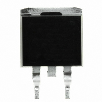
IRL1404ZSTRLPBF International Rectifier, IRL1404ZSTRLPBF Datasheet - Page 4

IRL1404ZSTRLPBF
Manufacturer Part Number
IRL1404ZSTRLPBF
Description
MOSFET N-CH 40V 75A D2PAK
Manufacturer
International Rectifier
Series
HEXFET®r
Specifications of IRL1404ZSTRLPBF
Fet Type
MOSFET N-Channel, Metal Oxide
Fet Feature
Logic Level Gate
Rds On (max) @ Id, Vgs
3.1 mOhm @ 75A, 10V
Drain To Source Voltage (vdss)
40V
Current - Continuous Drain (id) @ 25° C
75A
Vgs(th) (max) @ Id
2.7V @ 250µA
Gate Charge (qg) @ Vgs
110nC @ 5V
Input Capacitance (ciss) @ Vds
5080pF @ 25V
Power - Max
200W
Mounting Type
Surface Mount
Package / Case
D²Pak, TO-263 (2 leads + tab)
Transistor Polarity
N Channel
Continuous Drain Current Id
200A
Drain Source Voltage Vds
40V
On Resistance Rds(on)
2.5mohm
Rds(on) Test Voltage Vgs
10V
Threshold Voltage Vgs Typ
2.7V
Rohs Compliant
Yes
Lead Free Status / RoHS Status
Lead free / RoHS Compliant
Other names
IRL1404ZSTRLPBFTR
1000.00
100.00
100000
10.00
4
10000
1000
1.00
100
Fig 5. Typical Capacitance vs.
Fig 7. Typical Source-Drain Diode
0.0
1
Drain-to-Source Voltage
T J = 175°C
V DS , Drain-to-Source Voltage (V)
V SD , Source-to-Drain Voltage (V)
V GS = 0V,
C iss = C gs + C gd , C ds SHORTED
C rss = C gd
C oss = C ds + C gd
0.5
Forward Voltage
T J = 25°C
1.0
f = 1 MHZ
10
C oss
C rss
C iss
1.5
V GS = 0V
2.0
100
2.5
10000
1000
100
6.0
5.0
4.0
3.0
2.0
1.0
0.0
10
Fig 8. Maximum Safe Operating Area
1
1
0
Fig 6. Typical Gate Charge vs.
Tc = 25°C
Tj = 175°C
Single Pulse
I D = 75A
Gate-to-Source Voltage
V DS , Drain-to-Source Voltage (V)
Q G Total Gate Charge (nC)
20
OPERATION IN THIS AREA
LIMITED BY R DS (on)
10
V DS = 32V
V DS = 20V
40
10msec
1msec
100µsec
100
www.irf.com
60
1000
80


