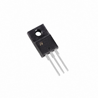
STF17NF25 STMicroelectronics, STF17NF25 Datasheet - Page 4

STF17NF25
Manufacturer Part Number
STF17NF25
Description
MOSFET N-CH 250V 17A TO-220FP
Manufacturer
STMicroelectronics
Series
STripFET™r
Datasheet
1.STF17NF25.pdf
(17 pages)
Specifications of STF17NF25
Fet Type
MOSFET N-Channel, Metal Oxide
Fet Feature
Standard
Rds On (max) @ Id, Vgs
165 mOhm @ 8.5A, 10V
Drain To Source Voltage (vdss)
250V
Current - Continuous Drain (id) @ 25° C
17A
Vgs(th) (max) @ Id
4V @ 250µA
Gate Charge (qg) @ Vgs
29.5nC @ 10V
Input Capacitance (ciss) @ Vds
1000pF @ 25V
Power - Max
25W
Mounting Type
Through Hole
Package / Case
TO-220-3 Full Pack (Straight Leads)
Transistor Polarity
N Channel
Continuous Drain Current Id
8.5A
Drain Source Voltage Vds
250V
On Resistance Rds(on)
140mohm
Rds(on) Test Voltage Vgs
10V
Threshold Voltage Vgs Typ
3V
Rohs Compliant
Yes
Configuration
Single
Resistance Drain-source Rds (on)
0.165 Ohms
Drain-source Breakdown Voltage
250 V
Gate-source Breakdown Voltage
+/- 20 V
Continuous Drain Current
17 A
Power Dissipation
25 W
Maximum Operating Temperature
+ 150 C
Mounting Style
Through Hole
Minimum Operating Temperature
- 55 C
Lead Free Status / RoHS Status
Lead free / RoHS Compliant
Other names
497-7471-5
STF17NF25
STF17NF25
Available stocks
Company
Part Number
Manufacturer
Quantity
Price
Company:
Part Number:
STF17NF25
Manufacturer:
ST
Quantity:
22 000
Company:
Part Number:
STF17NF25
Manufacturer:
ST
Quantity:
12 500
Electrical characteristics
2
4/17
Electrical characteristics
(T
Table 4.
Table 5.
1. Pulsed: pulse duration=300µs, duty cycle 1.5%
V
Symbol
Symbol
R
V
C
CASE
(BR)DSS
g
I
I
DS(on)
C
GS(th)
C
C
oss eq
Q
Q
DSS
GSS
R
fs
Q
oss
rss
iss
gs
gd
G
g
(1)
=25°C unless otherwise specified)
Drain-source breakdown
voltage
Zero gate voltage drain
current (V
Gate body leakage current
(V
Gate threshold voltage
Static drain-source on
resistance
Forward transconductance
Input capacitance
Output capacitance
Reverse transfer
capacitance
Equivalent output
capacitance
Total gate charge
Gate-source charge
Gate-drain charge
Gate input resistance
On/off states
Dynamic
DS
= 0)
Parameter
Parameter
GS
= 0)
STI17NF25 - STD17NF25 - STF17NF25 - STP17NF25
I
V
V
V
V
V
V
V
V
V
V
(see Figure 16)
f=1MHz gate DC bias=0 test
signal level=20mV open
drain
D
GS
GS
GS
GS
DS
DS
DS
DS
DS
DD
= 1mA, V
= V
= 10V, I
=0, V
=200V, I
= Max rating,
= Max rating,Tc=125°C
= ±20V
= 15V, I
=25V, f=1 MHz, V
=10V
Test conditions
Test conditions
GS
DS
, I
D
GS
D
D
=0V to 200V
D
= 8.5A
= 250µA
= 8.5A
= 17A
= 0
GS
=0
Min.
Min.
250
2
1000
Typ.
Typ.
0.14
29.5
15.6
178
135
4.8
14
28
3
2
0.165
Max.
Max.
±
100
10
1
4
Unit
Unit
nC
nC
nC
pF
pF
pF
pF
µA
µA
nA
S
Ω
V
V
Ω


