PCA9620H/Q900/1,51 NXP Semiconductors, PCA9620H/Q900/1,51 Datasheet
PCA9620H/Q900/1,51
Specifications of PCA9620H/Q900/1,51
Available stocks


Related parts for PCA9620H/Q900/1,51


PCA9620H/Q900/1,51 Summary of contents
Page 1
PCA9620 Universal LCD driver for low multiplex rates Rev. 1 — 9 December 2010 1. General description The PCA9620 is a peripheral device which interfaces to almost any Liquid Crystal Display 1 (LCD) LCD containing up to eight backplanes, 60 ...
Page 2
... NXP Semiconductors 3. Ordering information Table 1. Type number PCA9620H 4. Marking Table 2. Type number PCA9620H 5. Block diagram V LCD V DD2 V SS CLOCK SELECT TEMPERATURE SENSOR OSCILLATOR CLK SCL INPUT CONTROLLER FILTERS SDA (1) The charge pump can generate a maximum output voltage of 3 × V Fig 1. Block diagram of PCA9620 ...
Page 3
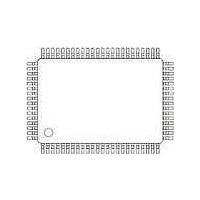
... NXP Semiconductors 6. Pinning information 6.1 Pinning Fig 2. Pin configuration for LQFP80 (PCA9620H) PCA9620 Product data sheet S20 1 S21 2 3 S22 4 S23 S24 5 S25 6 S26 7 8 S27 9 S28 S29 10 S30 11 S31 12 13 S32 14 S33 S34 15 S35 16 S36 17 18 S37 19 S38 S39 20 Top view. For mechanical details, see All information provided in this document is subject to legal disclaimers. Rev. 1 — ...
Page 4
... NXP Semiconductors 6.2 Pin description Table 3. Symbol S0 to S59 BP0 to BP7 V LCD V DD2 V DD1 CLK A0, A1 SCL SDA When the internal V [ output. When the external supply is requested then pin V supplied to it. In this case the internal charge pump must be disabled (see PCA9620 ...
Page 5
... NXP Semiconductors 7. Functional description The PCA9620 is a versatile peripheral device designed to interface any microprocessor or microcontroller to a wide variety of LCDs. It can directly drive any static or multiplexed LCD containing up to 480 elements. 7.1 Commands of PCA9620 The PCA9620 is controlled by 22 commands, which are defined in combinations of operation code bits that are not mentioned in this document may lead to undesired operation modes of PCA9620 ...
Page 6
... NXP Semiconductors Table 5. Bit 7.1.2 Command: OTP-refresh During production and testing of the device, each IC is calibrated in order to achieve the specified accuracy of V calibration is performed on EPROM cells called One Time Programmable (OTP) cells. These cells are being read by the device at power-on, after a reset, and every time when the initialize command or the OTP-refresh command is sent ...
Page 7
... NXP Semiconductors 7.1.4 Command: charge-pump-ctrl The charge-pump-ctrl command enables or disables the internal V controls the charge pump voltage multiplier setting. Table 8. Bit [1] Default value. 7.1.5 Command: temp-msr-ctrl The temp-msr-ctrl command enables or disables the temperature measurement block and the temperature compensation of V Table 9. ...
Page 8
... NXP Semiconductors Table 11. Bit [1] Default value. 7.1.7 Command: display-enable Table 12. Bit [1] Default value. 7.1.8 Command: set-MUX-mode Table 13. Bit [1] Default value. 7.1.9 Command: set-bias-mode Table 14. Bit [1] Default value. 7.1.10 Command: load-data-pointer The load-data-pointer command defines one of the 60 display RAM addresses where the following display data will be sent to ...
Page 9
... NXP Semiconductors Table 15. Bit 7.1.11 Command: frame-frequency With the frame-frequency command the frame frequency and the output clock frequency can be configured. Table 16. Bit Table 17. F[4:0] 00000 00001 00010 00011 00100 00101 00110 00111 01000 01001 01010 01011 01100 01101 [3] 01110 01111 ...
Page 10
... NXP Semiconductors 7.1.12 Bank select commands For multiplex drive modes 1:4, 1:2 and static drive mode possible to write data to one area of the RAM whilst displaying from another. These areas are named as RAM banks. Input and output banks can be set independently from one another with the input-bank-select and the output-bank-select command ...
Page 11
... NXP Semiconductors 7.1.13 Command: write-RAM-data The write-RAM-data command writes data byte-wise to the RAM. After Power-On Reset (POR) the RAM content is random and should be brought to a defined status by clearing it (setting it logic 0). Table 20. Bit [1] For this command bit RS of the control byte has to be set logic 1 (see More information about the display RAM can be found in 7 ...
Page 12
... NXP Semiconductors In frame inversion mode the DC value is compensated across two frames and not within one frame. Changing the inversion mode to frame inversion reduces the power consumption, therefore it is useful when power consumption is a key point in the application. Frame inversion may not be suitable for all applications. The RMS voltage across a segment is better defined, however since the switching frequency is reduced there is possibility for flicker to occur ...
Page 13
... NXP Semiconductors Fig 3. Table 24. Number of Backplanes All of the display configurations in shown in V DD1 V Fig 4. PCA9620 Product data sheet 7-segment with dot Example of displays suitable for PCA9620 Selection of possible display configurations Icons Digits/Characters 7-segment 480 60 320 45 240 30 120 Table 24 Figure 4 (internal V ) and in ...
Page 14
... NXP Semiconductors V DD1 V Fig 5. The host microprocessor or microcontroller maintains the 2 line I channel with the PCA9620. The appropriate biasing voltages for the multiplexed LCD waveforms are generated internally. The only other connections required to complete the system are the power supplies (V LCD panel selected for the application. ...
Page 15
... NXP Semiconductors 9. Temperature filter is disabled. 10. The internal V 11. The V 12. The display is disabled. Remark: Do not transfer data on the I the reset action to complete. The first command sent to the device after the power-on event must be the initialize command (see After Power-On Reset (POR) and before enabling the display, the RAM content should be brought to a defined status • ...
Page 16
... NXP Semiconductors 7.3.2 Recommended start-up sequences This chapter describes how to proceed with the initialization of the chip in different application modes. (1) This time depends on the external capacitor on pin V (2) RAM data may be written before or during the ramp- Fig 6. PCA9620 Product data sheet START ...
Page 17
... NXP Semiconductors Fig 7. (1) The external clock signal can be applied after the generation of the V (2) This time depends on the external capacitor on pin V (3) RAM data may be written before or during the ramp- Fig 8. PCA9620 Product data sheet START Power- DD1 DD2 and V ...
Page 18
... NXP Semiconductors Fig 9. 7.3.3 Recommended power-down sequences With the following sequences the PCA9620 can be set to a state of minimum power consumption, called power-down mode. Fig 10. Recommended power-down sequence for minimum power-down current when PCA9620 Product data sheet START Power- DD1 DD2 and V ...
Page 19
... NXP Semiconductors Fig 11. Recommended power-down sequence when using an external supplied V Fig 12. Recommended power-down sequence when using the internal charge pump and PCA9620 Product data sheet play by setting perature mea- the internal clock signal START Disable dis- play by setting bit E logic 0 Stop genera- ...
Page 20
... NXP Semiconductors Fig 13. Recommended power-down sequence when using an external supplied V Remark necessary to run the power-down sequence before removing the supplies. Depending on the application, care must be taken that no other signals are present at the chip input or output pins when removing the supplies (please refer to page 53) ...
Page 21
... NXP Semiconductors Table 26. LCD drive modes: summary of characteristics LCD drive Number of: mode Backplanes Levels static 1 2 1:2 multiplex 2 3 1:2 multiplex 2 4 [3] 1:2 multiplex 2 5 [3] 1:4 multiplex 4 3 1:4 multiplex 4 4 [3] 1:4 multiplex 4 5 [3] 1:6 multiplex 6 3 1:6 multiplex 6 4 1:6 multiplex ...
Page 22
... NXP Semiconductors V ( off RMS Discrimination is the ratio RMS --------------------- - V ( off RMS It should be noted that V 7.4.1.1 Electro-optical performance Suitable values for V RMS voltage, at which a pixel will be switched on or off, determine the transmissibility of the pixel. For any given liquid, there are two threshold values defined. One point relative ...
Page 23
... NXP Semiconductors 7.4.2 LCD drive mode waveforms 7.4.2.1 Static drive mode The static LCD drive mode is used when a single backplane is provided in the LCD. Fig 15. Static drive mode waveforms (line inversion mode) PCA9620 Product data sheet V LCD BP0 LCD LCD Sn (a) Waveforms at driver. ...
Page 24
... NXP Semiconductors 7.4.2.2 1:2 Multiplex drive mode When two backplanes are provided in the LCD, the 1:2 multiplex mode applies. The PCA9620 allows the use of Figure 17. Fig 16. Waveforms for the 1:2 multiplex drive mode with PCA9620 Product data sheet ⁄ ⁄ bias or ...
Page 25
... NXP Semiconductors Fig 17. Waveforms for the 1:2 multiplex drive mode with PCA9620 Product data sheet V LCD 2V /3 LCD BP0 V /3 LCD LCD 2V /3 LCD BP1 V /3 LCD LCD 2V /3 LCD LCD LCD 2V /3 LCD S n LCD LCD 2V /3 LCD V /3 LCD ...
Page 26
... NXP Semiconductors 7.4.2.3 1:4 Multiplex drive mode When four backplanes are provided in the LCD, the 1:4 multiplex drive mode applies, as shown in BP0 BP1 BP2 BP3 Sn Sn+1 Sn+2 Sn+3 state 1 state 2 Fig 18. Waveforms for the 1:4 multiplex drive mode with PCA9620 Product data sheet Figure 18 ...
Page 27
... NXP Semiconductors 7.4.2.4 1:6 Multiplex drive mode When six backplanes are provided in the LCD, the 1:6 multiplex drive mode applies. The PCA9620 allows the use of Figure 20. V LCD LCD BP0 LCD LCD LCD BP1 LCD LCD LCD BP2 LCD LCD LCD ...
Page 28
... NXP Semiconductors V LCD LCD BP0 LCD LCD LCD BP1 LCD LCD LCD BP2 LCD LCD LCD BP3 LCD LCD LCD BP4 LCD LCD LCD BP5 LCD LCD LCD LCD LCD LCD LCD LCD state − LCD − LCD −V LCD V LCD ...
Page 29
... NXP Semiconductors 7.4.2.5 1:8 Multiplex drive mode V LCD LCD BP0 LCD LCD LCD BP1 LCD LCD LCD BP2 LCD LCD LCD BP3 LCD LCD LCD BP4 LCD LCD LCD BP5 LCD LCD LCD BP6 LCD LCD LCD BP7 LCD LCD LCD ...
Page 30
... NXP Semiconductors V LCD 3/4 V LCD BP0 1/4 V LCD LCD 3/4 V LCD BP1 1/4 V LCD LCD 3/4 V LCD BP2 1/4 V LCD LCD 3/4 V LCD BP3 1/4 V LCD LCD 3/4 V LCD BP4 1/4 V LCD LCD 3/4 V LCD BP5 1/4 V LCD LCD 3/4 V LCD ...
Page 31
... NXP Semiconductors When eight backplanes are provided in the LCD, the 1:8 multiplex drive mode applies, as shown in 7.4.3 V generation LCD V can be generated and controlled on the chip by using software commands. When LCD the internal charge pump is used, the programmed V charge pump generates a V The charge pump can be enabled or disabled with the CPE bit (see With bit CPC the charge pump multiplier setting can be configured ...
Page 32
... NXP Semiconductors It has to be taken into account that the charge pump has to be configured (via bit CPC) properly to obtain the desired voltage range. For example × LCD Section configured with CPC set to 3 × LCD (1) V DD2 ( > 3.0 V then VPR[7:0] must be set so that V ...
Page 33
... NXP Semiconductors 7.4.5 Charge pump driving capability Figure 25 deliver. Fig 25. Charge pump model (used to characterize the driving strength) The output resistance of the charge pump is specified in values it can be calculated how much current the charge pump can drive under certain conditions. Example: Assuming the user would like to have the normal operation point at 25 °C with ...
Page 34
... NXP Semiconductors DD2 The ratio between these two numbers determines the charge pump power efficiency: η (1) η (2) η (3) V (4) V Fig 26. Power efficiency of the charge pump Loading the charge pump with higher currents decreases the output voltage. This decrease is determined by the charge pump driving capability, respectively by the output ...
Page 35
... NXP Semiconductors In case it is desired to change the charge pump frequency recommended to make a graph like basically imply to find out what would be the maximum V be the maximum load currents required. Then it can be decided which is the best setting of bit CPF. Tuning the charge pump frequency might be a difficult task to do and requires good knowledge of the application in which the IC is being used ...
Page 36
... NXP Semiconductors (°C) (1) Environment temperature, T1 (°C). (2) Measured temperature, T2 (°C). (3) Temperature deviation, Δ − T1. Fig 28. Temperature measurement delay This delay may cause undesired effects at start-up when the environment temperature may be different than the reset value of the PCA9620 which is 20 °C. In this case it takes till the correct measured temperature value will be available ...
Page 37
... NXP Semiconductors Table 29. SLA[2:0] to SLD[2:0] value [2] 000 001 010 011 100 101 110 111 [1] The relationship between the temperature coefficients and the slope factor is derived from the following equation: [2] Default value. The slope factors imply a linear correction, however the implementation is set in steps (parameter n in Fig 29 ...
Page 38
... NXP Semiconductors The V offset(LCD offset LCD Table 30. Temperature range T ≤ −40 °C −40 °C ≤ T ≤ −10 °C −10 °C < T ≤ 20 °C 20 °C < T ≤ 50 °C 50 °C < T < 80 °C 80 °C ≤ temperature compensation is possible above 80 °C. Above this value, the system maintains the [1] compensation value from 80 ° ...
Page 39
... NXP Semiconductors Remark: In case that a external clock is used then this clock signal must always be supplied to the device; removing the clock may freeze the LCD state, which is not suitable for the liquid crystal. Removal of the clock is possible when following the correct procedures. See 7 ...
Page 40
... NXP Semiconductors 7.7 Segment outputs The LCD drive section includes 60 segment outputs (S0 to S59) which must be connected directly to the LCD. The segment output signals are generated based on the multiplexed backplane signals and with data resident in the display register. When less than 60 segment outputs are required, the unused segment outputs must be left open-circuit ...
Page 41
... NXP Semiconductors Fig 30. Display RAM bitmap 7.9.1 Data pointer The addressing mechanism for the display RAM is realized using the data pointer. This allows the loading of an individual display data byte series of display data bytes into any location of the display RAM. The sequence commences with the initialization of the data pointer by the load-data-pointer command ...
Page 42
... NXP Semiconductors The data pointer is automatically incremented in accordance with the chosen LCD multiplex drive mode configuration. That is, after each byte is stored, the contents of the data pointer are incremented • by eight (static drive mode) • by four (1:2 multiplex drive mode) • by two (1:4 multiplex drive mode) • ...
Page 43
... NXP Semiconductors data pointer display RAM Fig 32. Discarded bits and data pointer wrap around at the end of data transmission 7.9.1.2 RAM filling in 1:2 multiplex drive mode In the 1:2 multiplex drive mode the eight transmitted data bits are placed in four successive display RAM columns of two rows (see ...
Page 44
... NXP Semiconductors display RAM rows/ backplane outputs Fig 35. Display RAM filling order in 1:4 multiplex drive mode In order to fill the whole four RAM rows 30 bytes need to be sent to the PCA9620. After the last byte sent, the data pointer is wrapped around to column 0 to start a possible RAM content update (see the data pointer, all the bits in the byte will be written correctly ...
Page 45
... NXP Semiconductors display RAM rows/ backplane outputs (BP) Fig 37. Display RAM filling order in 1:6 multiplex drive mode The remaining bits are wrapped up into the next column. In order to fill the whole RAM addresses 45 bytes need to be sent to the PCA9620. After the last byte sent the data ...
Page 46
... NXP Semiconductors display RAM rows/ backplane outputs Fig 39. Display RAM filling order in 1:8 multiplex drive mode In order to fill the whole RAM addresses 60 bytes need to be sent to the PCA9620. After the last byte sent the data pointer is wrapped around to column 0 to start a possible RAM content update (see transmitted data byte can be written over the RAM boundary ...
Page 47
... NXP Semiconductors INPUT-BANK-SELECT COMMAND CONTROLS THE INPUT DATA PATH Fig 41. Example of bank selection in 1:4 multiplex mode In Figure 41 read from the first four rows of the memory (bank 0), while the transmitted data is stored in the second four rows of the memory (bank 4) which is currently not accessed for the reading ...
Page 48
... NXP Semiconductors 7.9.2.2 Output-bank-select The output-bank-select command (see transferring it to the display register in accordance with the selected LCD drive configuration. • In the static drive mode it is possible to request the content of RAM bank 1 (row 1) to RAM bank 7 (row 7) for display instead of the default RAM bank 0 (row 0). ...
Page 49
... NXP Semiconductors C-bus interface characteristics 2 The I C-bus is for bidirectional, two-line communication between different ICs or modules. The two lines are a Serial DAta line (SDA) and a Serial CLock line (SCL). Both lines must be connected to a positive supply via a pull-up resistor when connected to the output stages of a device ...
Page 50
... NXP Semiconductors SDA SCL Fig 45. System configuration 8.4 Acknowledge The number of data bytes transferred between the START and STOP conditions from transmitter to receiver is unlimited. Each byte of eight bits is followed by an acknowledge cycle. • A slave receiver which is addressed must generate an acknowledge after the reception of each byte. • ...
Page 51
... NXP Semiconductors 2 8.5 I C-bus controller The PCA9620 acts transmit data acknowledge signals and the temperature readout byte of the selected device. 8.6 Input filters To enhance noise immunity in electrically adverse environments, RC low-pass filters are provided on the SDA and SCL lines. 2 8.7 I C-bus slave address ...
Page 52
... NXP Semiconductors 2 The I C-bus protocol is shown in condition (S) from the I addresses available. All PCA9620’s with the corresponding A1 and A0 level acknowledge in parallel to the slave address, but all PCA9620 with the alternative A1 and A0 levels ignore the whole I After acknowledgement, a control byte follows which defines if the next byte is RAM or command information ...
Page 53
... NXP Semiconductors 9. Internal circuitry Fig 50. Device protection diagram PCA9620 Product data sheet V DD1 A0, A1, T1, T2, CLK LCD BP0 to BP7 S59 V SS All information provided in this document is subject to legal disclaimers. Rev. 1 — 9 December 2010 PCA9620 Universal LCD driver for low multiplex rates ...
Page 54
... NXP Semiconductors 10. Limiting values CAUTION Static voltages across the liquid crystal display can build up when the LCD supply voltage (V LCD display artifacts. To avoid such artifacts, V Table 34. In accordance with the Absolute Maximum Rating System (IEC 60134). Symbol V DD1 V DD2 I DD1 I DD2 ...
Page 55
... NXP Semiconductors 11. Static characteristics Table 35. Static characteristics DD1 DD2 specified. Symbol Parameter Supplies V supply voltage 1 DD1 V supply voltage 2 DD2 V LCD supply voltage LCD ΔV LCD voltage variation LCD I power-down mode supply DD(pd) current I supply current 1 DD1 I supply current 2 DD2 ...
Page 56
... NXP Semiconductors Table 35. Static characteristics DD1 DD2 specified. Symbol Parameter 2 I C-bus; pins SDA and SCL V input voltage I V LOW-level input voltage IL V HIGH-level input voltage IH V output voltage O I LOW-level output current OL I leakage current L LCD outputs ΔV ...
Page 57
... NXP Semiconductors V (1) VPR[7:0] = 85h. (2) VPR[7:0] = 64h. (3) VPR[7:0] = A4h. Fig 51. Typical V I (μA) Fig 52. Typical I PCA9620 Product data sheet 8.3 LCD (V) 7.8 7.3 6.8 6.3 5.8 −50 0 Temperature compensation disabled. with respect to temperature LCD 120 DD1 100 80 60 − 5.0 V. DD1 ...
Page 58
... NXP Semiconductors I (μA) Fig 53. Typical I I (μA) Fig 54. Typical I PCA9620 Product data sheet 300 DD2 260 220 180 140 100 −40 0 Charge pump set to 2 × DD2 LCD with respect to temperature DD2 140 LCD 120 100 80 − 7.0 V, external supplied; V LCD ...
Page 59
... NXP Semiconductors 12. Dynamic characteristics Table 36. Dynamic characteristics DD1 DD2 specified. Symbol Parameter f oscillator frequency osc f external clock frequency clk(ext) t HIGH-level clock time clk(H) t LOW-level clock time clk(L) 2 Timing characteristics: I C-bus f SCL frequency SCL t bus free time between a BUF STOP and START condition ...
Page 60
... NXP Semiconductors Fig 55. Driver timing waveforms protocol SCL SDA Fig 56. I PCA9620 Product data sheet 1/f clk t clk(H) CLK START bit 7 condition MSB (S) (A7 SU;STA LOW HIGH BUF HD;STA SU;DAT 2 C-bus timing waveforms All information provided in this document is subject to legal disclaimers. ...
Page 61
... NXP Semiconductors 13. Package outline LQFP80: plastic low profile quad flat package; 80 leads; body 1 pin 1 index DIMENSIONS (mm are the original dimensions) A UNIT max. 0.16 1.5 mm 1.6 0.25 0.04 1.3 Note 1. Plastic or metal protrusions of 0.25 mm maximum per side are not included. OUTLINE VERSION ...
Page 62
... NXP Semiconductors 14. Soldering of SMD packages This text provides a very brief insight into a complex technology. A more in-depth account of soldering ICs can be found in Application Note AN10365 “Surface mount reflow soldering description”. 14.1 Introduction to soldering Soldering is one of the most common methods through which packages are attached to Printed Circuit Boards (PCBs), to form electrical circuits ...
Page 63
... NXP Semiconductors 14.4 Reflow soldering Key characteristics in reflow soldering are: • Lead-free versus SnPb soldering; note that a lead-free reflow process usually leads to higher minimum peak temperatures (see reducing the process window • Solder paste printing issues including smearing, release, and adjusting the process window for a mix of large and small components on one board • ...
Page 64
... NXP Semiconductors Fig 58. Temperature profiles for large and small components For further information on temperature profiles, refer to Application Note AN10365 “Surface mount reflow soldering description”. PCA9620 Product data sheet maximum peak temperature = MSL limit, damage level temperature minimum peak temperature = minimum soldering temperature MSL: Moisture Sensitivity Level All information provided in this document is subject to legal disclaimers ...
Page 65
... NXP Semiconductors 15. Abbreviations Table 39. Acronym AEC CDM DC EPROM ESD HBM LCD LSB MSB MSL MUX OTP PCB POR RC RAM RMS SCL SDA SMD PCA9620 Product data sheet Abbreviations Description Automotive Electronics Council Charged-Device Model Direct Current Erasable Programmable Read-Only Memory ElectroStatic Discharge ...
Page 66
... NXP Semiconductors 16. References [1] AN10365 — Surface mount reflow soldering description [2] AN10853 — ESD and EMC sensitivity of IC [3] IEC 60134 — Rating systems for electronic tubes and valves and analogous semiconductor devices [4] IEC 61340-5 — Protection of electronic devices from electrostatic phenomena [5] IPC/JEDEC J-STD-020D — Moisture/Reflow Sensitivity Classification for ...
Page 67
... NXP Semiconductors 17. Revision history Table 40. Revision history Document ID Release date PCA9620 v.1 20101209 PCA9620 Product data sheet Universal LCD driver for low multiplex rates Data sheet status Change notice Product data sheet - All information provided in this document is subject to legal disclaimers. Rev. 1 — 9 December 2010 ...
Page 68
... In no event shall NXP Semiconductors be liable for any indirect, incidental, punitive, special or consequential damages (including - without limitation - lost profits, lost savings, business interruption, costs related to the removal or ...
Page 69
... NXP Semiconductors Export control — This document as well as the item(s) described herein may be subject to export control regulations. Export might require a prior authorization from national authorities. 19. Contact information For more information, please visit: For sales office addresses, please send an email to: PCA9620 Product data sheet 18 ...
Page 70
... NXP Semiconductors 20. Contents 1 General description . . . . . . . . . . . . . . . . . . . . . . 1 2 Features and benefits . . . . . . . . . . . . . . . . . . . . 1 3 Ordering information . . . . . . . . . . . . . . . . . . . . . 2 4 Marking . . . . . . . . . . . . . . . . . . . . . . . . . . . . . . . . 2 5 Block diagram . . . . . . . . . . . . . . . . . . . . . . . . . . 2 6 Pinning information . . . . . . . . . . . . . . . . . . . . . . 3 6.1 Pinning . . . . . . . . . . . . . . . . . . . . . . . . . . . . . . . 3 6.2 Pin description . . . . . . . . . . . . . . . . . . . . . . . . . 4 7 Functional description . . . . . . . . . . . . . . . . . . . 5 7.1 Commands of PCA9620 . . . . . . . . . . . . . . . . . . 5 7.1.1 Command: initialize . . . . . . . . . . . . . . . . . . . . . 5 7.1.2 Command: OTP-refresh . . . . . . . . . . . . . . . . . . 6 7.1.3 Command: oscillator-ctrl . . . . . . . . . . . . . . . . . . 6 7.1.4 Command: charge-pump-ctrl ...
Page 71
... NXP Semiconductors 19 Contact information Contents . . . . . . . . . . . . . . . . . . . . . . . . . . . . . . 70 Universal LCD driver for low multiplex rates Please be aware that important notices concerning this document and the product(s) described herein, have been included in section ‘Legal information’. © NXP B.V. 2010. For more information, please visit: http://www.nxp.com For sales office addresses, please send an email to: salesaddresses@nxp ...