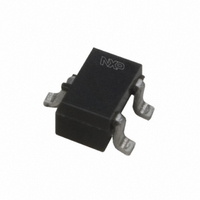
PMF370XN,115 NXP Semiconductors, PMF370XN,115 Datasheet

PMF370XN,115
Specifications of PMF370XN,115
PMF370XN T/R
PMF370XN T/R
Available stocks
Related parts for PMF370XN,115
PMF370XN,115 Summary of contents
Page 1
PMF370XN N-channel TrenchMOS extremely low level FET Rev. 03 — 20 June 2008 1. Product profile 1.1 General description Extremely low level N-channel enhancement mode Field-Effect Transistor (FET plastic package using TrenchMOS technology. This product is designed and ...
Page 2
... NXP Semiconductors 2. Pinning information Table 2. Pinning Pin Symbol Description 1 G gate 2 S source 3 D drain 3. Ordering information Table 3. Ordering information Type number Package Name Description PMF370XN SC-70 plastic surface-mounted package; 3 leads 4. Limiting values Table 4. Limiting values In accordance with the Absolute Maximum Rating System (IEC 60134). ...
Page 3
... NXP Semiconductors 120 I der (%) 100 × 100 % der 25°C ) Fig 1. Normalized continuous drain current as a function of solder point temperature Limit R (A) DSon 25° single pulse Fig 3. Safe operating area; continuous and peak drain currents as a function of drain-source voltage PMF370XN_3 Product data sheet ...
Page 4
... NXP Semiconductors 5. Thermal characteristics Table 5. Thermal characteristics Symbol Parameter R thermal resistance th(j-sp) from junction to solder point th(j-sp) (K/W) δ 0.2 0.1 0.05 0.02 10 single pulse Fig 4. Transient thermal impedance from junction to solder point as a function of pulse duration 6. Characteristics Table 6. Characteristics Symbol ...
Page 5
... NXP Semiconductors Table 6. Characteristics …continued Symbol Parameter R drain-source on-state DSon resistance Dynamic characteristics Q total gate charge G(tot) Q gate-source charge GS Q gate-drain charge GD C input capacitance iss C output capacitance oss C reverse transfer rss capacitance t turn-on delay time d(on) t rise time r t turn-off delay time ...
Page 6
... NXP Semiconductors (th) (V) 1.5 max 1 typ min 0.5 0 − 0.25 A Fig 7. Gate-source threshold voltage as a function of junction temperature 1 V ( DSon (Ω) 0.8 0.6 0.4 0 0 25°C j Fig 9. Drain-source on-state resistance as a function of drain current; typical values PMF370XN_3 Product data sheet ...
Page 7
... NXP Semiconductors GS(pl) V GS(th GS1 GS2 G(tot) Fig 11. Gate charge waveform definitions (pF − 0V Fig 13. Input, output and reverse transfer capacitances as a function of drain-source voltage; typical values PMF370XN_3 Product data sheet N-channel TrenchMOS extremely low level FET ( 003aaa508 I D Fig 12. Gate-source voltage as a function of gate charge ...
Page 8
... NXP Semiconductors 7. Package outline Plastic surface-mounted package; 3 leads DIMENSIONS (mm are the original dimensions UNIT max 1.1 0.4 0.25 mm 0.1 0.8 0.3 0.10 OUTLINE VERSION IEC SOT323 Fig 15. Package outline SOT323 (SC-70) PMF370XN_3 Product data sheet N-channel TrenchMOS extremely low level FET ...
Page 9
... NXP Semiconductors 8. Soldering 0.6 2.35 (3×) 0.55 (3×) Fig 16. SOT323 (SC-70) PMF370XN_3 Product data sheet N-channel TrenchMOS extremely low level FET 2.65 1.85 1.325 2 3 1.3 0.5 1 (3×) Rev. 03 — 20 June 2008 PMF370XN solder lands solder resist solder paste occupied area ...
Page 10
... Revision history Document ID Release date PMF370XN_3 20080620 • Modifications: The format of this data sheet has been redesigned to comply with the new identity guidelines of NXP Semiconductors. • Legal texts have been adapted to the new company name where appropriate PMF370XN_2 20051206 PMF370XN-01 20040211 PMF370XN_3 ...
Page 11
... Right to make changes — NXP Semiconductors reserves the right to make changes to information published in this document, including without limitation specifications and product descriptions, at any time and without notice ...
Page 12
... NXP Semiconductors 12. Contents 1 Product profile . . . . . . . . . . . . . . . . . . . . . . . . . . 1 1.1 General description . . . . . . . . . . . . . . . . . . . . . 1 1.2 Features and benefits . . . . . . . . . . . . . . . . . . . . 1 1.3 Applications . . . . . . . . . . . . . . . . . . . . . . . . . . . 1 1.4 Quick reference data . . . . . . . . . . . . . . . . . . . . 1 2 Pinning information . . . . . . . . . . . . . . . . . . . . . . 2 3 Ordering information . . . . . . . . . . . . . . . . . . . . . 2 4 Limiting values Thermal characteristics . . . . . . . . . . . . . . . . . . 4 6 Characteristics . . . . . . . . . . . . . . . . . . . . . . . . . . 4 7 Package outline . . . . . . . . . . . . . . . . . . . . . . . . . 8 8 Soldering . . . . . . . . . . . . . . . . . . . . . . . . . . . . . . 9 9 Revision history . . . . . . . . . . . . . . . . . . . . . . . . 10 10 Legal information ...


