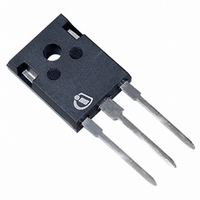
SPW11N60C3 Infineon Technologies, SPW11N60C3 Datasheet
SPW11N60C3
Specifications of SPW11N60C3
SPW11N60C3
SPW11N60C3IN
SPW11N60C3X
SPW11N60C3XK
Available stocks


Related parts for SPW11N60C3

SPW11N60C3 Summary of contents
Page 1
Gate source voltage static Rev. 2.6 Please note the new package dimensions arccording to PCN 2009-134 jmax ...
Page 2
wavesoldering Rev. 2.6 Please note the new package dimensions arccording to PCN 2009-134-A R thJC R thJA V (BR)DSS ...
Page 3
Transconductance Input capacitance Output capacitance Reverse transfer capacitance Turn-on delay time Rise time Turn-off delay time Fall time Gate to source charge Gate to drain charge 4 I <=I , di/dt<=400A/us DClink Identical low-side and high-side switch. ...
Page 4
Inverse diode direct current, pulsed Reverse recovery time Reverse recovery charge Peak reverse recovery current Rev. 2.6 Please note the new package dimensions arccording to PCN 2009-134 ...
Page 5
T C Rev. 2.6 Please note the new package dimensions arccording to PCN 2009-134 ...
Page 6
Rev. 2.6 Please note the new package dimensions arccording to PCN 2009-134 ...
Page 7
max V DS max di/ Rev. 2.6 Please note the new package dimensions arccording to PCN 2009-134 ...
Page 8
Rev. 2.6 Please note the new package dimensions arccording to PCN 2009-134-A dv/ ...
Page 9
(BR)DSS j Rev. 2.6 Please note the new package dimensions arccording to PCN 2009-134 ...
Page 10
iss C oss C rss Rev. 2.6 Please note the new package dimensions arccording to PCN 2009-134-A C oss ...
Page 11
G Rev. 2.6 Please note the new package dimensions arccording to PCN 2009-134 ...
Page 12
Rev. 2.6 Please note the new package dimensions arccording to PCN 2009-134 ...
Page 13
New package outlines TO-247 Assembly capacity extension for CoolMOSTM technology products assembled in lead-free package PG-TO247-3 at subcontractor ASE (Weihai) Inc., China (Changes are marked in blue.) Figure 1 Outlines TO-247, dimensions in mm/inches Final Data Sheet Erratum Data ...