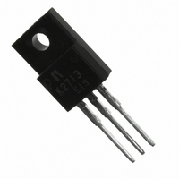
RDN120N25 Rohm Semiconductor, RDN120N25 Datasheet
Home Discrete Semiconductor Products MOSFETs, GaNFETs - Single RDN120N25
Manufacturer Part Number
RDN120N25
Description
MOSFET N-CH 250V 12A TO-220FN
Manufacturer
Rohm Semiconductor
Specifications of RDN120N25
Fet Type
MOSFET N-Channel, Metal Oxide
Fet Feature
Standard
Rds On (max) @ Id, Vgs
210 mOhm @ 6A, 10V
Drain To Source Voltage (vdss)
250V
Current - Continuous Drain (id) @ 25° C
12A
Vgs(th) (max) @ Id
4V @ 1mA
Gate Charge (qg) @ Vgs
62nC @ 10V
Input Capacitance (ciss) @ Vds
1224pF @ 10V
Power - Max
40W
Mounting Type
Through Hole
Package / Case
TO-220FN-3 (Straight Leads)
Lead Free Status / RoHS Status
Lead free / RoHS Compliant
Available stocks
Transistors
10V Drive Nch MOS FET
RDN120N25
Silicon N-channel
MOS FET
1) Low on-resistance.
2) Low input capacitance.
3) Exellent resistance to damage from static electricity.
Switching
∗1 Pw ≤ 10µs, Duty cycle ≤ 1%
∗2 L 2.4mH, V
Channel to case
Channel to ambient
Drain-Source Voltage
Gate-Source Voltage
Drain Current
Reverse Drain
Current
Source Current
(Body diode)
Avalanche Current
Avalanche Energy
Total Power Dissipation (T
Channel Temperature
Storage Temperature
Type
RDN120N25
Structure
Features
Application
Packaging specifications
Absolute maximum ratings (Ta=25°C)
Thermal resistance
Parameter
DD
=50V, R
Package
Code
Basic ordering unit (pieces)
Parameter
G
=25Ω, 1Pulse, Tch=25°C
Continuous
Pulsed
Continuous
Pulsed
Continuous
Pulsed
C
=25°C)
Symbol
Bulk
500
V
V
−
I
E
T
I
T
I
DRP
I
I
P
DSS
GSS
I
DR
I
DP
SP
AS
stg
D
S
AS
ch
D
∗1
∗1
∗1
∗2
∗2
Rth(ch-c)
Rth(ch-a)
Symbol
−55 to +150
Limits
250
±30
216
150
12
48
12
48
12
48
12
40
Limits
3.13
62.5
External dimensions (Unit : mm)
(1)Gate
(2)Drain
(3)Source
Unit
mJ
TO-220FN
°C
°C
W
V
V
A
A
A
A
A
A
A
°C/W
°C/W
Unit
∗A protection diode is included between the gate and
the source terminals to protect the diode against static
electricity when the product is in use. Use the protection
circuit when the fixed voltages are exceeded.
Equivalent circuit
∗1 ESD Protection diode
∗2 Body Diode
2.54
1.2
(1)
10.0
(2) (3)
Gate
2.54
1.3
0.8
φ 3.2
0.75
∗1
RDN120N25
Rev.A
4.5
Drain
Source
2.8
2.6
∗2
1/4
Related parts for RDN120N25
RDN120N25 Summary of contents
... °C T 150 ch −55 to +150 °C T stg Symbol Limits Rth(ch-c) 3.13 Rth(ch-a) 62.5 RDN120N25 10.0 4.5 φ 3.2 2.8 1.2 1.3 0.8 2.54 2.54 0.75 2.6 (1) (2) (3) Equivalent circuit Drain ∗2 Gate ∗1 ∗1 ESD Protection diode ∗2 Body Diode Source ∗ ...
... Q 11.0 gd Min. Typ. Max. Unit ∗ − − ∗ − − 169 12A ∗ − − µC di/dt= 100A / µs 0.95 RDN120N25 Unit Conditions ±10 µA = ±30V ⎯ =250µ µA =250V =10V, I =1mA V 4 Ω =6A, V =10V ...
... Ta= −25°C 10 Ta=25°C Ta=75°C 5 Ta=125° 0.5 0.2 0.05 0.1 0.2 0 DRAIN CURRENT : I (A) D Fig.8 Forward Transfer Admittance vs. Drain Current RDN120N25 100 =10V V DS Pulsed 10 Ta=125°C Ta=75°C Ta=25°C 1 Ta= −25°C 0.1 0. GATE-SOURCE VOLTAGE : V (V) GS Fig ...
... Single pulse 0.001 10µ 100µ 1m 10m 100m 1 10 PULSE WIDTH : PW (S) Fig.14 Normalized Transient Thermal Resistance vs. Pulse Width RDN120N25 1000 Ta=25° dt=100A / µs = Pulsed 100 10 0 100 REVERSE DRAIN CURRENT : I (A) DR Fig.12 Reverse Recovery Time vs. Reverse Drain Current Rev ...
Appendix No technical content pages of this document may be reproduced in any form or transmitted by any means without prior permission of ROHM CO.,LTD. The contents described herein are subject to change without notice. The specifications for the product ...
Related keywords
rdn120n25 RDN120N25 datasheet RDN120N25 data sheet RDN120N25 pdf datasheet RDN120N25 component RDN120N25 part RDN120N25 distributor RDN120N25 RoHS RDN120N25 datasheet download


