STW34NB20 STMicroelectronics, STW34NB20 Datasheet
STW34NB20
Specifications of STW34NB20
Available stocks


Related parts for STW34NB20


STW34NB20 Summary of contents
Page 1
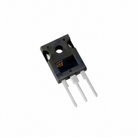
... POWER SUPPLIES AND MOTOR DRIVE HIGH CURRENT, HIGH SPEED SWITCHING ■ Table 2. Order Codes Part Number STW34NB20 N-CHANNEL 200V - 0.062 Ω - 34A TO-247 Figure 1. Package R I DS(on Figure 2. Internal Schematic Diagram Marking Package TO-247 W34NB20 STW34NB20 PowerMESH™ MOSFET TO-247 Packaging TUBE 1/10 ...
Page 2
... STW34NB20 Table 3. Absolute Maximum Ratings Symbol V Drain-source Voltage ( Drain- gate Voltage (R DGR V Gate-source Voltage GS I Drain Current (cont Drain Current (cont (1) Drain Current (pulsed Total Dissipation at T tot Derating Factor T Storage Temperature stg T Max. Operating Junction Temperature j Note: 1. Pulse width limited by safe operating area Table 4 ...
Page 3
... Test Conditions = 4.7 Ω 100 (see test circuit, Figure 16 160 Test Conditions = 4.7 Ω 160 (see test circuit, Figure 18) GS STW34NB20 Min. Typ. Max. Unit 200 V µA 1 µA 10 ± 100 nA Min. Typ. Max. Unit Ω 0.062 0.075 Min. Typ. Max. Unit 8 ...
Page 4
... STW34NB20 Table 11. Source Drain Diode Symbol Parameter I Source-drain Current SD (1) Source-drain Current I SDM (pulsed) (2) Forward On Voltage Reverse Recovery Time rr Q Reverse RecoveryCharge rr I Reverse RecoveryCharge RRAM Note: 1. Pulse width limited by safe operating area 2. Pulsed: Pulse duration = 300 µs, duty cycle 1.5 % Figure 3 ...
Page 5
... STW34NB20 PACKAGE MECHANICAL Table 12. TO-247 Mechanical Data Symbol Min A 4.85 A1 2.20 b 1.0 b1 2.0 b2 3.0 c 0.40 D 19.85 E 15. 14.20 L1 3.70 L2 ØP 3.55 ØR 4.50 S Figure 19. TO-247 Package Dimensions Note: Drawing is not to scale. 8/10 millimeters Typ Max 5.15 2.60 1.40 2.40 3.40 0.80 20 ...