IRF624 Vishay, IRF624 Datasheet
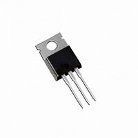
MOSFET N-CH 250V 4.4A TO-220AB

IRF624

Manufacturer Part Number
IRF624
Description
MOSFET N-CH 250V 4.4A TO-220AB
Manufacturer
Vishay
Datasheet

Specifications of IRF624

Fet Type
MOSFET N-Channel, Metal Oxide
Fet Feature
Standard
Rds On (max) @ Id, Vgs
1.1 Ohm @ 2.6A, 10V
Drain To Source Voltage (vdss)
250V
Current - Continuous Drain (id) @ 25° C
4.4A
Vgs(th) (max) @ Id
4V @ 250µA
Gate Charge (qg) @ Vgs
14nC @ 10V
Input Capacitance (ciss) @ Vds
260pF @ 25V
Power - Max
50W
Mounting Type
Through Hole
Package / Case
TO-220-3 (Straight Leads)
Configuration
Single
Transistor Polarity
N-Channel
Resistance Drain-source Rds (on)
1.1 Ohms
Drain-source Breakdown Voltage
250 V
Gate-source Breakdown Voltage
+/- 20 V
Continuous Drain Current
4.4 A
Power Dissipation
50 W
Maximum Operating Temperature
+ 150 C
Mounting Style
Through Hole
Minimum Operating Temperature
- 55 C
Lead Free Status / RoHS Status
Contains lead / RoHS non-compliant
Other names
*IRF624

Available stocks

Company
Part Number
Manufacturer
Quantity
Price
Part Number:
IRF624
Quantity:
4 710
Part Number:
IRF624A
Manufacturer:
IR
Quantity:
12 500
Part Number:
IRF624A
Manufacturer:
FAIRCHILD/仙童
Quantity:
20 000
Part Number:
IRF624B
Manufacturer:
FSC
Quantity:
2 000
Company:
Part Number:
IRF624PBF
Quantity:
15 934
Company:
Part Number:
IRF624PBF
Quantity:
70 000
Company:
Part Number:
IRF624SPBF
Quantity:
13 900
Notes
a. Repetitive rating; pulse width limited by maximum junction temperature (see fig. 11).
b. V
c. I
d. 1.6 mm from case.
* Pb containing terminations are not RoHS compliant, exemptions may apply
Document Number: 91029
S-82998-Rev. A, 12-Jan-09
PRODUCT SUMMARY
V
R
Q
Q
Q
Configuration
ORDERING INFORMATION
Package
Lead (Pb)-free
SnPb
ABSOLUTE MAXIMUM RATINGS T
PARAMETER
Drain-Source Voltage
Gate-Source Voltage
Continuous Drain Current
Pulsed Drain Current
Linear Derating Factor
Single Pulse Avalanche Energy
Repetitive Avalanche Current
Repetitive Avalanche Energy
Maximum Power Dissipation
Peak Diode Recovery dV/dt
Operating Junction and Storage Temperature Range
Soldering Recommendations (Peak Temperature)
Mounting Torque
DS
DS(on)
g
gs
gd
SD
DD
(Max.) (nC)
(nC)
(nC)
(V)
≤ 4.4 A, dI/dt ≤ 90 A/µs, V
= 50 V, starting T
(Ω)
TO-220
G
a
D
J
S
= 25 °C, L = 8.3 mH, R
c
a
a
DD
b
V
GS
≤ V
= 10 V
DS
G
, T
N-Channel MOSFET
J
Single
≤ 150 °C.
250
2.7
7.8
14
G
= 25 Ω, I
D
S
C
Power MOSFET
= 25 °C, unless otherwise noted
1.1
V
GS
AS
6-32 or M3 screw
at 10 V
= 4.4 A (see fig. 12).
T
for 10 s
C
= 25 °C
T
T
C
C
TO-220
IRF624PbF
SiHF624-E3
IRF624
SiHF624
= 100 °C
= 25 °C
FEATURES
• Dynamic dV/dt Rating
• Repetitive Avalanche Rated
• Fast Switching
• Ease of Paralleling
• Simple Drive Requirements
• Lead (Pb)-free Available
DESCRIPTION
Third generation Power MOSFETs from Vishay provide the
designer with the best combination of fast switching,
ruggedized
cost-effectiveness.
The TO-220 package is universally preferred for all
commercial-industrial applications at power dissipation
levels to approximately 50 W. The low thermal resistance
and low package cost of the TO-220 contribute to its wide
acceptance throughout the industry.
SYMBOL
T
dV/dt
J
V
V
E
E
I
I
P
, T
device
I
DM
AR
DS
GS
AS
AR
D
D
stg
design,
- 55 to + 150
IRF624, SiHF624
LIMIT
300
± 20
0.40
250
100
4.4
2.8
4.4
5.0
4.8
1.1
14
50
10
low
Vishay Siliconix
d
on-resistance
www.vishay.com
lbf · in
UNIT
W/°C
N · m
RoHS*
COMPLIANT
V/ns
mJ
mJ
°C
W
V
A
A
Available
and
1

Related parts for IRF624

IRF624 Summary of contents

Page 1

... TO-220 IRF624PbF SiHF624-E3 IRF624 SiHF624 = 25 °C, unless otherwise noted ° 100 ° °C C for screw = 25 Ω 4.4 A (see fig. 12 ≤ 150 °C. J IRF624, SiHF624 Vishay Siliconix device design, low on-resistance SYMBOL LIMIT V 250 DS V ± 4 2 0.40 E 100 AS I 4.4 ...

Page 2

... IRF624, SiHF624 Vishay Siliconix THERMAL RESISTANCE RATINGS PARAMETER Maximum Junction-to-Ambient Case-to-Sink, Flat, Greased Surface Maximum Junction-to-Case (Drain) SPECIFICATIONS °C, unless otherwise noted J PARAMETER Static Drain-Source Breakdown Voltage V Temperature Coefficient DS Gate-Source Threshold Voltage Gate-Source Leakage Zero Gate Voltage Drain Current Drain-Source On-State Resistance ...

Page 3

... Pulse Width Drain-to-Source Voltage ( 91029_02 Fig Typical Output Characteristics, T Document Number: 91029 S-82998-Rev. A, 12-Jan-09 4 ° 91029_03 = 25 ° 150 ° 91029_04 = 150 °C C IRF624, SiHF624 Vishay Siliconix 1 10 ° 150 ° µs Pulse Width Gate-to-Source Voltage ( Fig Typical Transfer Characteristics 3 4 ...

Page 4

... IRF624, SiHF624 Vishay Siliconix 600 MHz iss gs 500 rss oss ds 400 300 200 100 Drain-to-Source Voltage ( 91029_05 Fig Typical Capacitance vs. Drain-to-Source Voltage 4 125 Total Gate Charge (nC) 91029_06 G Fig Typical Gate Charge vs. Gate-to-Source Voltage www.vishay.com Shorted iss C oss C rss 1 91029_07 = 200 V DS ...

Page 5

... Fig. 12a - Unclamped Inductive Test Circuit Document Number: 91029 S-82998-Rev. A, 12-Jan-09 125 150 Single Pulse (Thermal Response Rectangular Pulse Duration ( IRF624, SiHF624 Vishay Siliconix D.U. Pulse width ≤ 1 µs Duty factor ≤ 0.1 % Fig. 10a - Switching Time Test Circuit ...

Page 6

... IRF624, SiHF624 Vishay Siliconix Fig. 12c - Maximum Avalanche Energy vs. Drain Current Charge Fig. 13a - Basic Gate Charge Waveform www.vishay.com 6 240 200 160 120 100 50 Starting T , Junction Temperature (°C) 91029_12c Top 2.0 A 2.8 A Bottom 4.4 A 125 150 Current regulator Same type as D.U.T. ...

Page 7

... R G • I controlled by duty factor SD P.W. Period D = Period P.W. waveform SD Body diode forward current dI/dt waveform DS Diode recovery dV/dt Body diode forward drop Ripple ≤ for logic level and 3 V drive devices Fig For N-Channel IRF624, SiHF624 Vishay Siliconix + + www.vishay.com 7 ...

Page 8

... Vishay disclaims any and all liability arising out of the use or application of any product described herein or of any information provided herein to the maximum extent permitted by law. The product specifications do not expand or otherwise modify Vishay’ ...

Related keywords