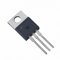
HUF75645P3 Fairchild Semiconductor, HUF75645P3 Datasheet - Page 2

HUF75645P3
Manufacturer Part Number
HUF75645P3
Description
MOSFET N-CH 100V 75A TO-220AB
Manufacturer
Fairchild Semiconductor
Series
UltraFET™r
Datasheet
1.HUF75645S3ST.pdf
(10 pages)
Specifications of HUF75645P3
Fet Type
MOSFET N-Channel, Metal Oxide
Fet Feature
Logic Level Gate
Rds On (max) @ Id, Vgs
14 mOhm @ 75A, 10V
Drain To Source Voltage (vdss)
100V
Current - Continuous Drain (id) @ 25° C
75A
Vgs(th) (max) @ Id
4V @ 250µA
Gate Charge (qg) @ Vgs
238nC @ 20V
Input Capacitance (ciss) @ Vds
3790pF @ 25V
Power - Max
310W
Mounting Type
Through Hole
Package / Case
TO-220-3 (Straight Leads)
Configuration
Single
Transistor Polarity
N-Channel
Resistance Drain-source Rds (on)
0.014 Ohm @ 10 V
Drain-source Breakdown Voltage
100 V
Gate-source Breakdown Voltage
+/- 20 V
Continuous Drain Current
75 A
Power Dissipation
310000 mW
Maximum Operating Temperature
+ 175 C
Mounting Style
Through Hole
Minimum Operating Temperature
- 55 C
Lead Free Status / RoHS Status
Lead free / RoHS Compliant
Available stocks
Company
Part Number
Manufacturer
Quantity
Price
Company:
Part Number:
HUF75645P3
Manufacturer:
ITS
Quantity:
800
Company:
Part Number:
HUF75645P3
Manufacturer:
FSC
Quantity:
5 000
Company:
Part Number:
HUF75645P3
Manufacturer:
FAIRCHILD
Quantity:
12 500
Company:
Part Number:
HUF75645P3 75A100V
Manufacturer:
FAIRCHILD
Quantity:
3 550
Electrical Specifications
Source to Drain Diode Specifications
©2001 Fairchild Semiconductor Corporation
OFF STATE SPECIFICATIONS
Drain to Source Breakdown Voltage
Zero Gate Voltage Drain Current
Gate to Source Leakage Current
ON STATE SPECIFICATIONS
Gate to Source Threshold Voltage
Drain to Source On Resistance
THERMAL SPECIFICATIONS
Thermal Resistance Junction to Case
Thermal Resistance Junction to
Ambient
SWITCHING SPECIFICATIONS (V
Turn-On Time
Turn-On Delay Time
Rise Time
Turn-Off Delay Time
Fall Time
Turn-Off Time
GATE CHARGE SPECIFICATIONS
Total Gate Charge
Gate Charge at 10V
Threshold Gate Charge
Gate to Source Gate Charge
Gate to Drain “Miller” Charge
CAPACITANCE SPECIFICATIONS
Input Capacitance
Output Capacitance
Reverse Transfer Capacitance
Source to Drain Diode Voltage
Reverse Recovery Time
Reverse Recovered Charge
PARAMETER
PARAMETER
T
GS
C
= 25
= 10V)
SYMBOL
SYMBOL
o
V
r
Q
BV
t
Q
DS(ON)
Q
C, Unless Otherwise Specified
t
d(OFF)
C
C
GS(TH)
R
R
I
I
d(ON)
t
g(TOT)
C
Q
Q
GSS
t
Q
V
DSS
OFF
g(TH)
g(10)
OSS
ON
RSS
ISS
t
DSS
t
t
SD
RR
gs
gd
r
rr
JC
f
JA
I
V
V
V
V
I
TO-220 and TO-263
V
V
R
(Figures 18, 19)
V
V
V
V
f = 1MHz
(Figure 12)
I
I
I
I
D
D
SD
SD
SD
SD
DS
DS
GS
GS
DD
GS
GS
GS
GS
GS
DS
= 250 A, V
= 75A, V
= 75A
= 35A
= 75A, dI
= 75A, dI
= 95V, V
= 90V, V
= 25V, V
= 20V
= V
= 50V, I
= 0V to 20V
= 0V to 10V
= 0V to 2V
= 2.5
10V,
DS
, I
GS
D
D
SD
SD
GS
GS
GS
GS
= 10V (Figure 9)
= 75A
TEST CONDITIONS
= 250 A (Figure 10)
TEST CONDITIONS
/dt = 100A/ s
/dt = 100A/ s
= 0V
= 0V, T
= 0V,
= 0V (Figure 11)
V
I
I
(Figures 13, 16, 17)
D
g(REF)
C
DD
= 75A,
= 150
= 50V,
= 1.0mA
o
C
MIN
100
MIN
2
-
-
-
-
-
-
-
-
-
-
-
-
-
-
-
-
-
-
-
-
-
-
-
-
HUF75645P3, HUF75645S3S Rev. B
0.0115
3790
TYP
117
198
106
810
230
TYP
6.8
14
41
97
14
41
-
-
-
-
-
-
-
-
-
-
-
-
-
0.014
MAX
MAX
0.48
1.25
1.00
250
197
207
238
127
145
360
8.2
100
62
1
4
-
-
-
-
-
-
-
-
-
-
UNITS
UNITS
o
o
C/W
C/W
nA
nC
nC
nC
nC
nC
pF
pF
pF
nC
ns
ns
ns
ns
ns
ns
ns
V
V
V
V
A
A


