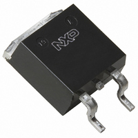
PHB45NQ10T,118 NXP Semiconductors, PHB45NQ10T,118 Datasheet - Page 6

PHB45NQ10T,118
Manufacturer Part Number
PHB45NQ10T,118
Description
MOSFET N-CH 100V 47A SOT404
Manufacturer
NXP Semiconductors
Series
TrenchMOS™r
Datasheet
1.PHB45NQ10T118.pdf
(12 pages)
Specifications of PHB45NQ10T,118
Package / Case
D²Pak, TO-263 (2 leads + tab)
Mounting Type
Surface Mount
Power - Max
150W
Fet Type
MOSFET N-Channel, Metal Oxide
Gate Charge (qg) @ Vgs
61nC @ 10V
Vgs(th) (max) @ Id
4V @ 1mA
Current - Continuous Drain (id) @ 25° C
47A
Drain To Source Voltage (vdss)
100V
Fet Feature
Standard
Rds On (max) @ Id, Vgs
25 mOhm @ 25A, 10V
Minimum Operating Temperature
- 55 C
Configuration
Single
Transistor Polarity
N-Channel
Resistance Drain-source Rds (on)
0.0085 Ohm @ 10 V
Drain-source Breakdown Voltage
75 V
Gate-source Breakdown Voltage
+/- 20 V
Continuous Drain Current
75 A
Power Dissipation
230000 mW
Maximum Operating Temperature
+ 175 C
Mounting Style
SMD/SMT
Lead Free Status / RoHS Status
Lead free / RoHS Compliant
Lead Free Status / RoHS Status
Lead free / RoHS Compliant, Lead free / RoHS Compliant
Other names
934055802118::PHB45NQ10T /T3::PHB45NQ10T /T3
Available stocks
Company
Part Number
Manufacturer
Quantity
Price
Part Number:
PHB45NQ10T,118
Manufacturer:
NEXPERIA/安世
Quantity:
20 000
NXP Semiconductors
PHB45NQ10T
Product data sheet
Fig 6.
Fig 8.
Fig 10. Normalized drain-source on-state resistance
(A)
(A)
I
I
a
D
D
2.9
2.1
1.3
0.5
40
30
20
10
50
40
30
20
10
0
0
−60
function of drain-source voltage; typical values
function of gate-source voltage; typical values
factor as a function of junction temperature
T
Output characteristics: drain current as a
V
Transfer characteristics: drain current as a
0
0
j
DS
= 25 °C
> I
D
0.4
x R
DSon
20
2
0.8
V
8
6
GS
T
j
= 175 °C
(V) = 10
1.2
100
4
V
1.6
T
T
All information provided in this document is subject to legal disclaimers.
GS
j
j
014aab206
014aab208
014aab210
(°C)
4.8
= 25 °C
4.6
4.4
V
5
4
(V)
DS
4.2
(V)
180
2
6
Rev. 02 — 8 July 2010
Fig 7.
Fig 9.
Fig 11. Gate-source threshold voltage as a function of
R
V
DS(on)
GS(th)
(Ω)
(S)
(V)
g
0.16
0.12
0.08
0.04
fs
50
40
30
20
10
0
0
5
4
3
2
1
0
-60
0
of drain current; typical values
drain current; typical values
junction temperature
T
Drain-source on-state resistance as a function
V
Forward transconductance as a function of
I
0
D
j
4 4.2
DS
N-channel TrenchMOS standard level FET
= 25 °C
= 1 mA; V
> I
D
10
4
x R
4.4
DSon
DS
20
= V
20
4.6
8
maximum
GS
minimum
PHB45NQ10T
typical
12
30
4.8
100
T
T
j
j
= 25 °C
= 175 °C
V
GS
© NXP B.V. 2010. All rights reserved.
T
16
40
j
014aab207
014aab209
014aab211
(°C)
(V) = 10
I
I
D
D
(A)
(A)
6
8
5
180
20
50
6 of 12


