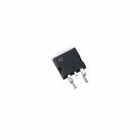
STB16NS25T4 STMicroelectronics, STB16NS25T4 Datasheet
STB16NS25T4
Specifications of STB16NS25T4
Available stocks


Related parts for STB16NS25T4


STB16NS25T4 Summary of contents
Page 1
... EXTREMELY HIGH dv/dt CAPABILITY 100% AVALANCHE TESTED DESCRIPTION Using the latest high voltage MESH OVERLAY™ process, STMicroelectronics has designed an ad- vanced family of power MOSFETs with outstanding performance. The new patented STrip layout cou- pled with the Company’s proprietary edge termina- tion structure, makes it suitable in coverters for lighting applications ...
Page 2
STB16NS25 THERMAL DATA Rthj-case Thermal Resistance Junction-case Max Rthj-amb Thermal Resistance Junction-ambient Max T Maximum Lead Temperature For Soldering Purpose l AVALANCHE CHARACTERISTICS Symbol I Avalanche Current, Repetitive or Not-Repetitive AR (pulse width limited Single Pulse Avalanche ...
Page 3
ELECTRICAL CHARACTERISTICS (CONTINUED) SWITCHING ON Symbol Parameter t Turn-on Delay Time d(on) t Rise Time r Q Total Gate Charge g Q Gate-Source Charge gs Q Gate-Drain Charge gd SWITCHING OFF Symbol Parameter t Turn-off- Delay Time d(off) Fall Time ...
Page 4
STB16NS25 Output Characteristics Transconductance Gate Charge vs Gate-source Voltage 4/9 Transfer Characteristics Static Drain-source On Resistance Capacitance Variations ...
Page 5
Normalized Gate Thereshold Voltage vs Temp. Source-drain Diode Forward Characteristics Normalized On Resistance vs Temperature Normalized BVDSS vs Temperature STB16NS25 5/9 ...
Page 6
STB16NS25 Fig. 1: Unclamped Inductive Load Test Circuit Fig. 3: Switching Times Test Circuit For Resistive Load Fig. 5: Test Circuit For Inductive Load Switching And Diode Recovery Times 6/9 Fig. 2: Unclamped Inductive Waveform Fig. 4: Gate Charge test ...
Page 7
D mm. DIM. MIN. TYP A 4.4 A1 2.49 A2 0.03 B 0.7 B2 1.14 C 0.45 C2 1. 8 1.27 L3 1.4 M 2.4 R 0.4 V2 ...
Page 8
STB16NS25 2 D PAK FOOTPRINT TAPE AND REEL SHIPMENT (suffix ”T4”)* TAPE MECHANICAL DATA mm inch DIM. MIN. MAX. MIN. A0 10.5 10.7 0.413 0.421 B0 15.7 15.9 0.618 0.626 D 1.5 1.6 0.059 0.063 D1 1.59 1.61 0.062 0.063 ...
Page 9
... No license is granted by implication or otherwise under any patent or patent rights of STMicroelectronics. Specifications mentioned in this publication are subject to change without notice. This publication supersedes and replaces all information previously supplied ...