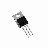
IRFB4229PBF International Rectifier, IRFB4229PBF Datasheet - Page 4

IRFB4229PBF
Manufacturer Part Number
IRFB4229PBF
Description
MOSFET N-CH 250V 46A TO-220AB
Manufacturer
International Rectifier
Series
HEXFET®r
Type
Power MOSFETr
Datasheet
1.IRFB4229PBF.pdf
(8 pages)
Specifications of IRFB4229PBF
Fet Type
MOSFET N-Channel, Metal Oxide
Fet Feature
Standard
Rds On (max) @ Id, Vgs
46 mOhm @ 26A, 10V
Drain To Source Voltage (vdss)
250V
Current - Continuous Drain (id) @ 25° C
46A
Vgs(th) (max) @ Id
5V @ 250µA
Gate Charge (qg) @ Vgs
110nC @ 10V
Input Capacitance (ciss) @ Vds
4560pF @ 25V
Power - Max
330W
Mounting Type
Through Hole
Package / Case
TO-220-3 (Straight Leads)
Transistor Polarity
N Channel
Continuous Drain Current Id
46A
Drain Source Voltage Vds
250V
On Resistance Rds(on)
38mohm
Rds(on) Test Voltage Vgs
10V
Threshold Voltage Vgs Typ
5V
Rohs Compliant
Yes
Number Of Elements
1
Polarity
N
Channel Mode
Enhancement
Drain-source On-res
0.046Ohm
Drain-source On-volt
250V
Gate-source Voltage (max)
±30V
Continuous Drain Current
46A
Power Dissipation
330W
Operating Temp Range
-40C to 175C
Operating Temperature Classification
Automotive
Mounting
Through Hole
Pin Count
3 +Tab
Package Type
TO-220AB
Drain-source Breakdown Voltage
250 V
Gate-source Breakdown Voltage
30 V
Mounting Style
Through Hole
Gate Charge Qg
72 nC
Lead Free Status / RoHS Status
Lead free / RoHS Compliant
Available stocks
Company
Part Number
Manufacturer
Quantity
Price
Company:
Part Number:
IRFB4229PBF
Manufacturer:
IR
Quantity:
3 000
Part Number:
IRFB4229PBF
Manufacturer:
IR
Quantity:
20 000
Fig 9. Typical Capacitance vs.Drain-to-Source Voltage
Fig 11. Maximum Drain Current vs. Case Temperature
2000
1600
1200
4
800
400
7000
6000
5000
4000
3000
2000
1000
50
40
30
20
10
0
0
0
Fig 7. Typical E
25
25
1
L = 220nH
C= 0.3µF
C= 0.2µF
C= 0.1µF
Crss
Coss
Ciss
50
50
V DS , Drain-to-Source Voltage (V)
T J , Junction Temperature (°C)
V GS = 0V,
C iss = C gs + C gd , C ds SHORTED
C rss = C gd
C oss = C ds + C gd
Temperature (°C)
75
10
75
PULSE
100
f = 1 MHZ
vs.Temperature
100
125
100
125
150
150
175
1000
Fig 10. Typical Gate Charge vs.Gate-to-Source Voltage
Fig 8. Typical Source-Drain Diode Forward Voltage
Fig 12. Maximum Safe Operating Area
1000
1000
100
0.1
100
0.1
20
16
12
10
10
8
4
0
1
1
0.2
0
1
I D = 26A
Tc = 25°C
Tj = 175°C
Single Pulse
V DS , Drain-to-Source Voltage (V)
20
V SD , Source-to-Drain Voltage (V)
T J = 175°C
0.4
Q G Total Gate Charge (nC)
OPERATION IN THIS AREA
LIMITED BY R DS (on)
40
10
V DS = 160V
V DS = 100V
V DS = 40V
100µsec
0.6
60
T J = 25°C
0.8
100
80
www.irf.com
V GS = 0V
1.0
100
10µsec
1µsec
1000
120
1.2


