IRFBA1405P International Rectifier, IRFBA1405P Datasheet

MOSFET N-CH 55V 174A SUPER-220

IRFBA1405P

Manufacturer Part Number
IRFBA1405P
Description
MOSFET N-CH 55V 174A SUPER-220
Manufacturer
International Rectifier
Series
HEXFET®r
Datasheet

Specifications of IRFBA1405P

Fet Type
MOSFET N-Channel, Metal Oxide
Fet Feature
Standard
Rds On (max) @ Id, Vgs
5 mOhm @ 101A, 10V
Drain To Source Voltage (vdss)
55V
Current - Continuous Drain (id) @ 25° C
174A
Vgs(th) (max) @ Id
4V @ 250µA
Gate Charge (qg) @ Vgs
260nC @ 10V
Input Capacitance (ciss) @ Vds
5480pF @ 25V
Power - Max
330W
Mounting Type
Through Hole
Package / Case
Super-220™-3 (Straight Leads)
Lead Free Status / RoHS Status
Contains lead / RoHS non-compliant
Other names
*IRFBA1405P
Q1429145

Available stocks

Company
Part Number
Manufacturer
Quantity
Price
Part Number:
IRFBA1405P
Manufacturer:
IR
Quantity:
20 000
Part Number:
IRFBA1405P
Manufacturer:
IR
Quantity:
3 000
Benefits
Description
Typical Applications
Specifically designed for Automotive applications, this Stripe Planar
design of HEXFET
techniques to achieve extremely low on-resistance per silicon area.
Additional features of this MOSFET are a 175
temperature, fast switching speed and improved ruggedness in
single and repetitive avalanche. The Super-220
has been designed to have the same mechanical outline and pinout
as the industry standard TO-220 but can house a considerably
larger silicon die. The result is significantly increased current
handling capability over both the TO-220 and the much larger TO-
247 package. The combination of extremely low on-resistance
silicon and the Super-220
component count in multiparalled TO-220 applications, reduce
system power dissipation, upgrade existing designs or have TO-247
performance in a TO-220 outline. This package has been designed
to meet automotive, Q101, qualification standard.
These benefits make this design an extremely efficient and reliable
device for use in Automotive applications and a wide variety of other
applications.
I
I
I
P
V
E
I
E
dv/dt
T
T
www.irf.com
D
D
DM
AR
J
STG
D
GS
AS
AR
@ T
@ T
Electric Power Steering (EPS)
Anti-lock Braking System (ABS)
Wiper Control
Climate Control
Power Door
@T
Advanced Process Technology
Ultra Low On-Resistance
Dynamic dv/dt Rating
175°C Operating Temperature
Fast Switching
Repetitive Avalanche Allowed up to Tjmax
C
C
C
= 25°C
= 100°C
= 25°C
®
Power MOSFETs utilizes the latest processing
Continuous Drain Current, V
Pulsed Drain Current 
Power Dissipation
Linear Derating Factor
Gate-to-Source Voltage
Single Pulse Avalanche Energy‚
Avalanche Current
Repetitive Avalanche Energy‡
Peak Diode Recovery dv/dt ƒ
Operating Junction and
Storage Temperature Range
Soldering Temperature, for 10 seconds
Recommended clip force
TM
package makes it ideal to reduce the
Parameter
AUTOMOTIVE MOSFET
o
C junction operating
TM
GS
GS
is a package that
@ 10V
@ 10V
G
See Fig.12a, 12b, 15, 16
300 (1.6mm from case )
HEXFET
IRFBA1405P
-40 to + 175
-55 to + 175
D
S
174†
123†
Max.
680
330
± 20
560
2.2
5.0
20
®
R
Power MOSFET
DS(on)
I
V
D
DSS
= 174A†
= 5.0m
= 55V
Units
W/°C
V/ns
°C
mJ
mJ
W
N
A
V
A
1

Related parts for IRFBA1405P

IRFBA1405P Summary of contents
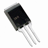
Page 1

... J T Storage Temperature Range STG Soldering Temperature, for 10 seconds Recommended clip force www.irf.com AUTOMOTIVE MOSFET junction operating package that @ 10V GS @ 10V GS See Fig.12a, 12b, 15, 16 IRFBA1405P ® HEXFET Power MOSFET 55V DSS R = 5.0m DS(on 174A† Max. Units 174† 123† ...

Page 2

Electrical Characteristics @ T Parameter V Drain-to-Source Breakdown Voltage (BR)DSS Breakdown Voltage Temp. Coefficient (BR)DSS J R Static Drain-to-Source On-Resistance DS(on) V Gate Threshold Voltage GS(th) g Forward Transconductance fs I Drain-to-Source Leakage Current DSS Gate-to-Source Forward ...

Page 3

VGS TOP 15V 10V 8.0V 7.0V 6.0V 5.5V 5.0V BOTTOM 4.5V 100 10 4.5V 20µs PULSE WIDTH 0 Drain-to-Source Voltage (V) DS Fig 1. Typical Output Characteristics 1000 ° T ...

Page 4

0V MHZ C iss = rss = oss = 10000 Ciss Coss 1000 Crss 100 1 ...

Page 5

LIMITED BY PACKAGE 160 120 100 125 T , Case Temperature ( C) C Fig 9. Maximum Drain Current Vs. Case Temperature 0.50 0.20 0.1 0.10 0.05 0.02 SINGLE PULSE ...

Page 6

D.U 20V 0. Fig 12a. Unclamped Inductive Test Circuit V (BR)DSS Fig 12b. Unclamped Inductive Waveforms Charge Fig 13a. ...

Page 7

Duty Cycle = Single Pulse 0.01 100 0. 1.0E-08 1.0E-07 Fig 15. Typical Avalanche Current Vs.Pulsewidth 600 TOP Single Pulse BOTTOM 10% Duty Cycle 500 101A 400 300 200 100 ...

Page 8

D.U.T + ‚ -  Driver Gate Drive P.W. D.U.T. I Waveform SD Reverse Recovery Current D.U. Re-Applied Voltage Inductor Curent For N-channel 8 + ƒ - „ - P.W. Period D = Period Body Diode Forward Current ...

Page 9

A 1.50 [.059] 0.50 [.020 4.00 [.157] 3.50 [.138] 2.55 [.100] 2X NOT ES: 1. DIMENS IONING & T OLERANCING PER AS ME Y14.5M-1994. 2. CONT ROLLING DIMENSION: MILLIMET ER. 3. DIMENS IONS ARE SHOWN IN MILLIMET ...

Related keywords