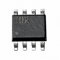
IRF7453TRPBF International Rectifier, IRF7453TRPBF Datasheet

IRF7453TRPBF
Specifications of IRF7453TRPBF
IRF7453TRPBF
IRF7453TRPBFTR
Related parts for IRF7453TRPBF
IRF7453TRPBF Summary of contents
Page 1
Applications High frequency DC-DC converters l Lead-Free l Benefits Low Gate to Drain Charge to Reduce l Switching Losses Fully Characterized Capacitance Including l Effective C to Simplify Design (See OSS App. Note AN1001) Fully Characterized Avalanche Voltage l and ...
Page 2
IRF7453PbF Static @ T = 25°C (unless otherwise specified) J Parameter V Drain-to-Source Breakdown Voltage (BR)DSS ∆V Breakdown Voltage Temp. Coefficient /∆T (BR)DSS J R Static Drain-to-Source On-Resistance DS(on) V Gate Threshold Voltage GS(th) I Drain-to-Source Leakage Current DSS Gate-to-Source ...
Page 3
VGS TOP 15V 12V 10V 8.0V 7.0V 6.0V 10 5.5V BOTTOM 5.0V 1 5.0V 0.1 20µs PULSE WIDTH 0.01 0 Drain-to-Source Voltage (V) DS Fig 1. Typical Output Characteristics 100 ...
Page 4
IRF7453PbF 10000 0V MHZ C iss = rss = oss = Ciss 1000 Coss Crss 100 10 ...
Page 5
T , Case Temperature ( C) C Fig 9. Maximum Drain Current Vs. Ambient Temperature 100 D = 0.50 0.20 10 0.10 0.05 0.02 1 0.01 0.1 SINGLE PULSE (THERMAL ...
Page 6
IRF7453PbF 0.26 0.24 0. 10V 0.20 0. Drain Current (A) Fig 12. On-Resistance Vs. Drain Current Current Regulator Same Type as D.U.T. V 50KΩ GS .2µF 12V .3µ ...
Page 7
SO-8 Package Outline Dimensions are shown in milimeters (inches 0.25 [.010] NOT DIMENS IONING & T OLERANCING PER AS ME Y14.5M-1994. 2. CONT ROLLING DIMENS ...
Page 8
IRF7453PbF SO-8 Tape and Reel Dimensions are shown in milimeters (inches) NOTES: 1. CONTROLLING DIMENSION : MILLIMETER. 2. ALL DIMENSIONS ARE SHOWN IN MILLIMETERS(INCHES). 3. OUTLINE CONFORMS TO EIA-481 & EIA-541. NOTES : 1. CONTROLLING DIMENSION : MILLIMETER. 2. OUTLINE ...


