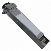
FTLX1412M3BCL Finisar Corporation, FTLX1412M3BCL Datasheet - Page 7

FTLX1412M3BCL
Manufacturer Part Number
FTLX1412M3BCL
Description
TX/RX Optical Fiber 11300Mbps 30-Pin XFP
Manufacturer
Finisar Corporation
Type
TX/RXr
Datasheet
1.FTLX1412M3BCL.pdf
(11 pages)
Specifications of FTLX1412M3BCL
Package
30XFP
Mounting
Snap Fit To Panel
Wavelength
1330(Max)/1600(Max) nm
Rise Time
0.038 ns
Operating Supply Voltage
3.13 to 3.45 V
Data Rate
11.3Gbps
Applications
Ethernet
Voltage - Supply
3.13 V ~ 3.45 V
Connector Type
LC Duplex
Mounting Type
XFP
Lead Free Status / RoHS Status
Lead free / RoHS Compliant
Other names
775-1048
Available stocks
Company
Part Number
Manufacturer
Quantity
Price
Company:
Part Number:
FTLX1412M3BCL
Manufacturer:
FINISAR
Quantity:
4
FTLX1412M3BCL Multirate XFP Product Specification – September 2007
VIII. Digital Diagnostic Functions
As defined by the XFP MSA
functions via a 2-wire serial interface, which allows real-time access to the following
operating parameters:
It also provides a sophisticated system of alarm and warning flags, which may be used to
alert end-users when particular operating parameters are outside of a factory-set normal
range.
The operating and diagnostics information is monitored and reported by a Digital
Diagnostics Transceiver Controller (DDTC) inside the transceiver, which is accessed
through the 2-wire serial interface. When the serial protocol is activated, the serial clock
signal (SCL pin) is generated by the host. The positive edge clocks data into the XFP
transceiver into those segments of its memory map that are not write-protected. The
negative edge clocks data from the XFP transceiver. The serial data signal (SDA pin) is
bi-directional for serial data transfer. The host uses SDA in conjunction with SCL to
mark the start and end of serial protocol activation. The memories are organized as a
series of 8-bit data words that can be addressed individually or sequentially. The 2-wire
serial interface provides sequential or random access to the 8 bit parameters, addressed
from 000h to the maximum address of the memory.
For more detailed information including memory map definitions, please see Finisar
Application Note AN-2035 “Digital Diagnostic Monitoring Interface for XFP Optical
Transceivers”, or the XFP MSA Specification
© Finisar Corporation 13-September-07
• Transceiver temperature
• Laser bias current
• Transmitted optical power
• Received optical power
• Transceiver supply voltage
1
, Finisar XFP transceivers provide digital diagnostic
Rev B
1
.
F i n i s a r
Page 7


