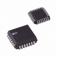
DAC8412FPC Analog Devices Inc, DAC8412FPC Datasheet

DAC8412FPC
Specifications of DAC8412FPC
Available stocks
Related parts for DAC8412FPC
DAC8412FPC Summary of contents
Page 1
FEATURES + ±15 V operation Unipolar or bipolar operation True voltage output Double-buffered inputs Reset to minimum (DAC8413) or center scale (DAC8412) Fast bus access time Readback APPLICATIONS Automatic test equipment Digitally controlled calibration Servo controls Process control ...
Page 2
DAC8412/DAC8413 TABLE OF CONTENTS Features .............................................................................................. 1 Applications ....................................................................................... 1 Functional Block Diagram .............................................................. 1 General Description ......................................................................... 1 Revision History ............................................................................... 2 Specifications ..................................................................................... 3 Electrical Characteristics ............................................................. 3 Absolute Maximum Ratings ............................................................ 7 Thermal Resistance ...................................................................... 7 ESD ...
Page 3
SPECIFICATIONS ELECTRICAL CHARACTERISTICS V = +15 −15 +5 LOGIC Table 1. Parameter ACCURACY Integral Nonlinearity Error Differential Nonlinearity Error Min-Scale Error Full-Scale Error Min-Scale Temperature Coefficient Full-Scale Temperature Coefficient Linearity ...
Page 4
DAC8412/DAC8413 Parameter SUPPLY CHARACTERISTICS Power Supply Sensitivity Positive Supply Current Negative Supply Current Power Dissipation 1 All supplies can be varied ±5%, and operation is guaranteed. Device is tested with nominal supplies. 2 Operation is guaranteed over this reference range, ...
Page 5
Parameter Write Data Setup Write Data Hold Load Data Pulse Width Reset Pulse Width Chip Select Read Pulse Width Read Data Hold Read Data Setup Data to High-Z Chip Select to Data SUPPLY CHARACTERISTICS Power Supply Sensitivity Positive Supply Current ...
Page 6
DAC8412/DAC8413 80ns R ADDRESS ADDRESS ADDRESS ADDRESS ONE TWO THREE t LS LDAC t WDS DATA1 DATA2 DATA3 DATA IN VALID VALID VALID Figure 5. Single-Buffer Mode R/W ADDRESS ADDRESS FOUR t ...
Page 7
ABSOLUTE MAXIMUM RATINGS T = +25°C, unless otherwise noted. A Table 3. Parameter Rating −0.3 V, +33 −0.3 V, +33 LOGIC V to DGND −0.3 V, +7.0 V LOGIC ...
Page 8
DAC8412/DAC8413 PIN CONFIGURATION AND FUNCTION DESCRIPTIONS REFH REFL OUTB OUTC OUTA OUTD DGND V 5 DAC8412/ 24 LOGIC RESET CS DAC8413 6 ...
Page 9
TYPICAL PERFORMANCE CHARACTERISTICS V = +15V –15V –10V REFL T = 25° – (V) REFH Figure 10. DNL vs. V REFH 1 0 –1 1 ...
Page 10
DAC8412/DAC8413 0.2 0 –0.2 DAC A DAC D –0.4 –0.6 –75 0 TEMPERATURE (°C) Figure 16. Full-Scale Error vs. Temperature 0.2 0 DAC A –0.2 DAC D DAC B –0.4 –0.6 –75 0 TEMPERATURE (°C) Figure 17. Zero-Scale Error vs. ...
Page 11
EA TRIG'D 0V –580ns 1µs/DIV Figure 22. Positive Slew Rate 15.5mV 0 INPUT –5V 2mV/DIV 5V/DIV TRIG'D –4.5mV –1.96µs 2µs/DIV Figure 23. Settling Time (Negative) 32.5mV 5V INPUT 0 5mV/DIV 1 LSB ERROR BAND 5V/DIV TRIG'D –17.5mV –1.96µs ...
Page 12
DAC8412/DAC8413 +15V –15V +10V 10 REFH V = –10V REFL T = 25° 0.01 0.1 1 LOAD RESISTANCE (kΩ) Figure 28. Output Swing vs. Load ...
Page 13
CH1 MEAN 66.19µ REFH V REFL T A 20µV/DIV M 200µs A CH1 Figure 34. Broadband Noise +15V +10V REFH ...
Page 14
DAC8412/DAC8413 THEORY OF OPERATION INTRODUCTION The DAC8412/DAC8413 are quad, voltage output, 12-bit parallel input DACs featuring a 12-bit data bus with readback capability. The only differences between the DAC8412/DAC8413 are the reset functions. The DAC8412 resets to midscale (Code 0x800), ...
Page 15
RESET The RESET function can be used either at power- any time during DAC operation. The RESET function is independent This pin is active low and sets the DAC output registers to either center code ...
Page 16
DAC8412/DAC8413 R/W DB11..DB0 V LOGIC READBACK DATAOUT_DB11 DGND Careful attention to grounding is important for accurate operation of the DAC8412. This is not because the DAC8412 is more sensitive than other 12-bit DACs, but because with four ...
Page 17
The 0.2 μF bypass capacitors shown at the reference inputs in Figure 40 should be used whenever ±10 V references are used. Applications with single references or references to ±5 V may not require the 0.2 μF bypassing. The 6.2 ...
Page 18
DAC8412/DAC8413 OUTLINE DIMENSIONS 0.458 (11.63) 0.442 (11.23 0.100 (2.54) BSC 0.250 (6.35) MAX 0.200 (5.08) 0.115 (2.92) 0.022 (0.56) 0.014 (0.36) 0.070 (1.78) 0.050 (1.27) CONTROLLING DIMENSIONS ARE IN INCHES; MILLIMETER DIMENSIONS (IN PARENTHESES) ARE ROUNDED-OFF INCH EQUIVALENTS ...
Page 19
PIN 1 0.042 (1.07) IDENTIFIER 0.050 TOP VIEW (1.27) (PINS DOWN) BSC 0.456 (11.582) SQ 0.120 (3.04) 0.450 (11.430) 0.090 (2.29) 0.495 ...
Page 20
... DAC8412FPC −40°C to +85°C 1 DAC8412FPC-REEL −40°C to +85° DAC8412FPCZ −40°C to +85°C DAC8412FPCZ-REEL 1, 2 −40°C to +85° DAC8412FPZ −40°C to +85°C DAC8413AT/883C −55°C to +125°C DAC8413BT/883C −55°C to +125°C DAC8413BTC/883C − ...


