MRF6V12500HR3 Freescale Semiconductor, MRF6V12500HR3 Datasheet
MRF6V12500HR3
Specifications of MRF6V12500HR3
Available stocks


Related parts for MRF6V12500HR3

MRF6V12500HR3 Summary of contents
Page 1
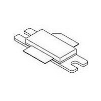
... LATERAL N- -CHANNEL RF POWER MOSFETs CASE 465- -06, STYLE 1 NI- -780 MRF6V12500HR3 CASE 465A- -06, STYLE 1 NI- -780S MRF6V12500HSR3 Symbol Value Unit V --0.5, +110 Vdc DSS V --6.0, +10 Vdc +150 °C stg T 150 ° 225 °C J (2,3) Symbol Value Unit Z 0.044 °C/W θJC MRF6V12500HR3 MRF6V12500HSR3 1 ...
Page 2
... Typical Broadband Performance — 960- -1215 MHz (In Freescale 960--1215 MHz Test Fixture, 50 ohm system 200 mA 500 W Peak (50 W Avg.), f = 960--1215 MHz, Pulsed, 128 μsec Pulse Width, 10% Duty Cycle DQ out Power Gain Drain Efficiency 1. Part internally matched both on input and output. MRF6V12500HR3 MRF6V12500HSR3 2 = 25°C unless otherwise noted) A Symbol I GSS V (BR)DSS ...
Page 3
... Z8 0.095″ x 1.710″ Microstrip Z9, Z20 0.482″ x 0.050″ Microstrip Z10 0.138″ x 1.500″ Microstrip Figure 1. MRF6V12500HR3(HSR3) Test Circuit Schematic Table 5. MRF6V12500HR3(HSR3) Test Circuit Component Designations and Values Part C1, C2 5.1 pF Chip Capacitors C3, C4, C5 Chip Capacitors C7, C10 10 μ Chip Capacitors C8, C11, C13, C16 2.2 μ ...
Page 4
... MRF6V12500H Rev C11 C10 R4 Figure 2. MRF6V12500HR3(HSR3) Test Circuit Component Layout MRF6V12500HR3 MRF6V12500HSR3 C14 C12 C15 C13 C2 C16 RF Device Data Freescale Semiconductor ...
Page 5
... P = 500 W out = 200 DUTY CYCLE (%) Figure 4. Safe Operating Area Ideal Actual Vdc 200 mA 1030 MHz DD DQ Pulse Width = 128 μsec, Duty Cycle = 10 INPUT POWER (dBm) PULSED in Input Power 100 , OUTPUT POWER (WATTS) PULSED out Output Power MRF6V12500HR3 MRF6V12500HSR3 25 42 1000 5 ...
Page 6
... Vdc, I 100 DD DQ Pulse Width = 128 μsec, Duty Cycle = 10 INPUT POWER (dBm) PULSED in Figure 9. Pulsed Output Power versus Input Power MRF6V12500HR3 MRF6V12500HSR3 6 TYPICAL CHARACTERISTICS --30_C --30_C C 20 85_C 25_C 25_C 19 18 55_C 85_C 17 16 η 200 mA 1030 MHz Figure 10. Pulsed Power Gain and Drain Efficiency ...
Page 7
... Z source MHz Ω 1030 1.36 -- j1.27 2.50 -- j0. Test circuit impedance as measured from source gate to ground Test circuit impedance as measured from load drain to ground. Device Input Matching Under Test Network Z Z source load Z load Ω Output Matching Network MRF6V12500HR3 MRF6V12500HSR3 7 ...
Page 8
... Chip Capacitors C13, C14 0.022 μF, 100 V Chip Capacitors C15, C16 0.10 μF, 100 V Chip Capacitors C17, C18 470 μ Electrolytic Capacitors R1 Ω, 1/4 W Chip Resistors PCB 0.030″, ε = 2.55 r MRF6V12500HR3 MRF6V12500HSR3 Description Part Number ATC100B2R2JT500XT ATC100B0R2BT500XT ATC100B330JT500XT G2225X7R225KT3AB T491X226K035AT ...
Page 9
... MHz = 200 mA 1150 MHz DQ η D 1150 MHz G ps 1030 MHz 250 300 350 400 450 500 P , PEAK OUTPUT POWER (WATTS) out Output Power --5 --10 --15 --20 1250 1300 65 60 960 MHz 55 1030 MHz 50 960 MHz 45 1215 MHz 40 550 600 MRF6V12500HR3 MRF6V12500HSR3 9 ...
Page 10
... MHz Figure 16. Series Equivalent Source and Load Impedance — 960- -1215 MHz MRF6V12500HR3 MRF6V12500HSR3 1215 MHz Z source Z load f = 960 MHz f = 960 MHz Vdc 200 mA 500 W Peak DD DQ out source load MHz Ω Ω 960 2.25 -- j1.78 1.38 -- j1.53 1030 2.51 -- j1.02 1 ...
Page 11
... U ------ 0.030 ------ 0.76 Z aaa 0.005 REF 0.127 REF bbb 0.010 REF 0.254 REF F ccc 0.015 REF 0.381 REF STYLE 1: PIN 1. DRAIN 2. GATE 5. SOURCE MRF6V12500HR3 MRF6V12500HSR3 MAX 34.16 9.91 4.32 12.83 1.14 0.15 1.70 5.33 19.96 20.00 3.51 9.53 9.52 11 ...
Page 12
... Fig. 13, Test Circuit Component Layout and Table 6, Test Circuit Component Designations and Values Fig. 14, Pulsed Power Gain, Drain Efficiency and IRL versus Frequency Fig. 15, Power Gain and Drain Efficiency versus Output Power Fig. 16, Series Equivalent Source and Load Impedance MRF6V12500HR3 MRF6V12500HSR3 12 REVISION HISTORY Description from --0 ...
Page 13
... Semiconductor was negligent regarding the design or manufacture of the part. Freescalet and the Freescale logo are trademarks of Freescale Semiconductor, Inc. All other product or service names are the property of their respective owners. © Freescale Semiconductor, Inc. 2009--2010. All rights reserved. MRF6V12500HR3 MRF6V12500HSR3 13 ...