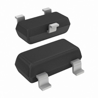
BFT93,215 NXP Semiconductors, BFT93,215 Datasheet - Page 4

BFT93,215
Manufacturer Part Number
BFT93,215
Description
TRANS PNP 12V 5GHZ SOT-23
Manufacturer
NXP Semiconductors
Datasheet
1.BFT93215.pdf
(10 pages)
Specifications of BFT93,215
Package / Case
SOT-23-3, TO-236-3, Micro3™, SSD3, SST3
Transistor Type
PNP
Voltage - Collector Emitter Breakdown (max)
12V
Frequency - Transition
5GHz
Noise Figure (db Typ @ F)
2.4dB @ 500MHz
Power - Max
300mW
Dc Current Gain (hfe) (min) @ Ic, Vce
20 @ 30mA, 5V
Current - Collector (ic) (max)
35mA
Mounting Type
Surface Mount
Dc Collector/base Gain Hfe Min
50
Minimum Operating Temperature
- 65 C
Mounting Style
SMD/SMT
Configuration
Single
Transistor Polarity
NPN
Maximum Operating Frequency
5 GHz
Collector- Emitter Voltage Vceo Max
- 12 V
Emitter- Base Voltage Vebo
- 2 V
Continuous Collector Current
- 35 mA
Power Dissipation
300 mW
Number Of Elements
1
Collector-emitter Voltage
12V
Collector-base Voltage
15V
Emitter-base Voltage
2V
Collector Current (dc) (max)
35mA
Dc Current Gain (min)
20
Frequency (max)
5GHz
Operating Temp Range
-65C to 175C
Operating Temperature Classification
Military
Mounting
Surface Mount
Pin Count
3
Package Type
TO-236AB
Dc
08+
Lead Free Status / RoHS Status
Lead free / RoHS Compliant
Gain
-
Lead Free Status / Rohs Status
Lead free / RoHS Compliant
Other names
568-1993-2
933347740215
BFT93 T/R
933347740215
BFT93 T/R
NXP Semiconductors
CHARACTERISTICS
T
Notes
1. G
2. d
November 1992
I
h
f
C
C
C
G
F
V
SYMBOL
j
CBO
T
FE
= 25 C unless otherwise specified.
o
PNP 5 GHz wideband transistor
c
e
re
UM
V
V
V
measured at f
G
im
p
q
r
UM
= V
UM
= V
= V
= 60 dB (DIN 45004B); I
is the maximum unilateral power gain, assuming S
o
o
o
=
6 dB; f
at d
6 dB; f
collector cut-off current
DC current gain
transition frequency
collector capacitance
emitter capacitance
feedback capacitance
maximum unilateral power gain
(note 1)
noise figure
output voltage
10 log
im
(pqr
= 60 dB; f
r
q
--------------------------------------------------------- - dB.
= 505.25 MHz;
PARAMETER
1
= 503.25 MHz;
) = 493.25 MHz.
–
S
11
S
p
2
1
21
= 495.25 MHz;
C
2
–
= 30 mA; V
S
22
2
I
I
I
f = 500 MHz
I
I
I
I
f = 500 MHz; T
I
f = 500 MHz; T
see Fig.2 and note 2
E
C
C
E
c
C
C
C
CE
= i
= 0; V
= i
= 30 mA; V
= 30 mA; V
= 2 mA; V
= 30 mA; V
= 10 mA; V
c
e
= 5 V; R
= 0; V
= 0; V
CB
CONDITIONS
= 5 V
EB
CB
4
CE
12
L
= 0.5 V; f = 1 MHz
amb
amb
CE
CE
CE
CE
= 10 V; f = 1 MHz
= 75 ;
is zero and
= 5 V; f = 1 MHz
= 5 V
= 5 V;
= 5 V;
= 5 V;
= 25 C
= 25 C
20
MIN.
50
5
0.95
1.8
1
16.5
2.4
300
TYP.
Product specification
50
MAX.
BFT93
nA
GHz
pF
pF
pF
dB
dB
mV
UNIT


