XC2VP7-5FFG672C Xilinx Inc, XC2VP7-5FFG672C Datasheet - Page 96
XC2VP7-5FFG672C
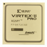
Manufacturer Part Number
XC2VP7-5FFG672C
Description
FPGA Virtex-II Pro™ Family 11088 Cells 1050MHz 0.13um/90nm (CMOS) Technology 1.5V 672-Pin FCBGA
Manufacturer
Xilinx Inc
Series
Virtex™-II Pror
Datasheet
1.XC2VP20-5FGG676C.pdf
(430 pages)
Specifications of XC2VP7-5FFG672C
Package
672FCBGA
Family Name
Virtex-II ProÂ
Device Logic Units
11088
Number Of Registers
9856
Maximum Internal Frequency
1050 MHz
Typical Operating Supply Voltage
1.5 V
Maximum Number Of User I/os
396
Ram Bits
811008
Number Of Logic Elements/cells
11088
Number Of Labs/clbs
1232
Total Ram Bits
811008
Number Of I /o
396
Voltage - Supply
1.425 V ~ 1.575 V
Mounting Type
Surface Mount
Operating Temperature
0°C ~ 85°C
Package / Case
672-BBGA, FCBGA
Lead Free Status / RoHS Status
Lead free / RoHS Compliant
Number Of Gates
-
Lead Free Status / RoHS Status
Lead free / RoHS Compliant
Other names
122-1370
Available stocks
Company
Part Number
Manufacturer
Quantity
Price
Company:

Part Number:
XC2VP7-5FFG672C
Manufacturer:
XILINX
Quantity:
745


IOB Output Switching Characteristics
Output delays terminating at a pad are specified for LVCMOS25 with 12 mA drive and fast slew rate. For other standards,
adjust the delays with the values shown in
Table 34: IOB Output Switching Characteristics
DS083 (v4.7) November 5, 2007
Product Specification
Notes:
1. A Zero “0” Hold Time listing indicates no hold time or a negative hold time. Negative values can not be guaranteed “best-case”, but
2. The 3-state turn-off delays should not be adjusted.
Propagation Delays
3-State Delays
Sequential Delays
Setup and Hold Times Before/After Clock CLK
Set/Reset Delays
O input to Pad
O input to Pad via transparent latch
T input to Pad high-impedance
T input to valid data on Pad
T input to Pad high-impedance via
transparent latch
T input to valid data on Pad via transparent latch
GTS to Pad high-impedance
Clock CLK to Pad
Clock CLK to Pad high-impedance (synchronous)
Clock CLK to valid data on Pad (synchronous)
O input
OCE input
SR input (OFF)
3–State Setup Times, T input
3-State Setup Times, TCE input
3-State Setup Times, SR input (TFF)
Minimum Pulse Width, SR inputs (asynchronous)
SR input to Pad (asynchronous)
SR input to Pad high-impedance (asynchronous)
SR input to valid data on Pad (asynchronous)
GSR to Pad
if a “0” is listed, there is no positive hold time.
R
(2)
Description
(2)
(2)
Virtex-II Pro and Virtex-II Pro X Platform FPGAs: DC and Switching Characteristics
IOB Output Switching Characteristics Standard
(2)
(2)
T
T
T
T
www.xilinx.com
IOOCECK
IOSRCKO
IOSRCKT
IOTCECK
T
T
IOOCK
IOTCK
T
T
Symbol
T
T
T
T
T
T
T
T
T
IOTLPON
IOTLPHZ
T
IOGSRQ
T
IOCKON
T
IOSRON
IOCKHZ
IOSRHZ
T
IOCKP
IOSRP
IOOLP
IOTHZ
IOOP
IOTP
RPW
GTS
/T
/T
/T
/T
/T
/T
IOCKO
IOCKOCE
IOCKOSR
IOCKT
IOCKTCE
IOCKTSR
0.23/ 0.12
0.39/ 0.01
0.52/ 0.00
0.23/ 0.12
0.39/ 0.01
0.52/ 0.00
1.58
1.65
1.23
1.51
1.08
1.56
4.11
1.59
1.39
1.67
0.37
2.33
1.97
2.24
5.87
-7
Speed Grade
0.26/ 0.14
0.44/ 0.01
0.57/ 0.00
0.26/ 0.14
0.44/ 0.01
0.57/ 0.00
1.68
1.82
1.35
1.63
1.22
1.69
4.73
1.76
1.55
1.82
0.40
2.56
2.16
2.44
6.75
Adjustments.
-6
0.29/ 0.15
0.49/ 0.01
0.75/ 0.00
0.29/ 0.15
0.49/ 0.01
0.75/ 0.00
1.85
1.99
1.51
1.78
1.36
1.85
5.20
1.93
1.73
2.00
0.45
2.83
2.41
2.69
7.43
-5
Module 3 of 4
ns, max
ns, max
ns, max
ns, max
ns, max
ns, max
ns, max
ns, max
ns, max
ns, max
ns, max
ns, max
ns, max
ns, max
ns, min
ns, min
ns, min
ns, min
ns, min
ns, min
ns, min
Units
25
Related parts for XC2VP7-5FFG672C
Image
Part Number
Description
Manufacturer
Datasheet
Request
R

Part Number:
Description:
IC FPGA VIRTEX-II PRO 896-FBGA
Manufacturer:
Xilinx Inc
Datasheet:
Part Number:
Description:
IC FPGA VIRTEX-II PRO 456-FBGA
Manufacturer:
Xilinx Inc
Datasheet:
Part Number:
Description:
IC FPGA VIRTEX-II PRO 456-FBGA
Manufacturer:
Xilinx Inc
Datasheet:

Part Number:
Description:
IC VIRTEXIIPRO FPGA 11K 672FBGA
Manufacturer:
Xilinx Inc
Datasheet:
Part Number:
Description:
IC FPGA VIRTEX-II PRO 672-FBGA
Manufacturer:
Xilinx Inc
Datasheet:
Part Number:
Description:
IC FPGA VIRTEX-II PRO 896-FBGA
Manufacturer:
Xilinx Inc
Datasheet:
Part Number:
Description:
IC FPGA VIRTEX-II PRO 896-FBGA
Manufacturer:
Xilinx Inc
Datasheet:
Part Number:
Description:
IC FPGA VIRTEX-II PRO 456-FBGA
Manufacturer:
Xilinx Inc
Datasheet:
Part Number:
Description:
IC FPGA VIRTEX-II PRO 456-FBGA
Manufacturer:
Xilinx Inc
Datasheet:
Part Number:
Description:
IC FPGA VIRTEX-II PRO 672-FBGA
Manufacturer:
Xilinx Inc
Datasheet:
Part Number:
Description:
IC FPGA VIRTEX-II PRO 672-FBGA
Manufacturer:
Xilinx Inc
Datasheet:
Part Number:
Description:
IC FPGA VIRTEX-II PRO 896-FBGA
Manufacturer:
Xilinx Inc
Datasheet:
Part Number:
Description:
IC FPGA VIRTEX-II PRO 896-FBGA
Manufacturer:
Xilinx Inc
Datasheet:
Part Number:
Description:
IC FPGA VIRTEX-II PRO 672FFBGA
Manufacturer:
Xilinx Inc
Datasheet:
Part Number:
Description:
IC FPGA VIRTEX-II PRO 672FFBGA
Manufacturer:
Xilinx Inc
Datasheet: