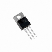
MJE13007G ON Semiconductor, MJE13007G Datasheet - Page 5

MJE13007G
Manufacturer Part Number
MJE13007G
Description
TRANS PWR NPN 8A 400V TO220AB
Manufacturer
ON Semiconductor
Series
SWITCHMODE™r
Type
Powerr
Specifications of MJE13007G
Transistor Type
NPN
Current - Collector (ic) (max)
8A
Voltage - Collector Emitter Breakdown (max)
400V
Vce Saturation (max) @ Ib, Ic
3V @ 2A, 8A
Current - Collector Cutoff (max)
100µA
Dc Current Gain (hfe) (min) @ Ic, Vce
5 @ 5A, 5V
Power - Max
80W
Frequency - Transition
14MHz
Mounting Type
Through Hole
Package / Case
TO-220-3 (Straight Leads)
Transistor Polarity
NPN
Mounting Style
Through Hole
Collector- Emitter Voltage Vceo Max
400 V
Emitter- Base Voltage Vebo
9 V
Maximum Dc Collector Current
8 A
Power Dissipation
80 W
Maximum Operating Temperature
+ 150 C
Continuous Collector Current
8 A
Dc Collector/base Gain Hfe Min
8
Maximum Operating Frequency
14 MHz
Minimum Operating Temperature
- 65 C
Current, Collector
8 A
Current, Gain
30
Frequency
14 MHz
Package Type
TO-220AB
Polarity
NPN
Primary Type
Si
Resistance, Thermal, Junction To Case
1.56 °C/W
Voltage, Breakdown, Collector To Emitter
400 V
Voltage, Collector To Emitter
400 V
Voltage, Collector To Emitter, Saturation
3 V
Voltage, Emitter To Base
9 V
Number Of Elements
1
Collector-emitter Voltage
400V
Emitter-base Voltage
9V
Collector Current (dc) (max)
8A
Dc Current Gain (min)
8
Frequency (max)
14MHz
Operating Temp Range
-65C to 150C
Operating Temperature Classification
Military
Mounting
Through Hole
Pin Count
3 +Tab
Lead Free Status / RoHS Status
Lead free / RoHS Compliant
Other names
MJE13007GOS
INTRODUCTION
transistor for SWITCHMODE applications are voltage and
current ratings, switching speed, and energy handling
capability. In this section, these specifications will be
discussed and related to the circuit examples illustrated in
Table 2. (Note 1)
VOLTAGE REQUIREMENTS
important in SWITCHMODE applications.
require high blocking voltage capability. In both circuits the
switching transistor is subjected to voltages substantially
higher than V
line diagrams at I
capability at this point depends on the base to emitter
conditions and the device junction temperature. Since the
highest device capability occurs when the base to emitter
junction is reverse biased (V
and specified use condition. Maximum I
is specified at a relatively low reverse bias (1.5 Volts) both
The primary considerations when selecting a power
Both blocking voltage and sustaining voltage are
Circuits B and C in Table 2 illustrate applications that
CC
after the device is completely off (see load
C
= I
SPECIFICATION INFORMATION FOR SWITCHMODE APPLICATIONS
leakage
CEV
≈ 0 in Table 2). The blocking
), this is the recommended
CEV
at rated V
http://onsemi.com
CEV
5
NOTE: 1. For detailed information on specific switching applications,
at 25°C and 100°C. Increasing the reverse bias will give
some improvement in device blocking capability.
switching applications occur during turn−on and turn−off. If
the load contains a significant capacitive component, high
current and voltage can exist simultaneously during turn−on
and the pulsed forward bias SOA curves (Figure 6) are the
proper design limits.
sustained simultaneously during turn−off, in most cases,
with the base to emitter junction reverse biased. Under these
conditions the collector voltage must be held to a safe level
at or below a specific value of collector current. This can be
accomplished by several means such as active clamping, RC
snubbing, load line shaping, etc. The safe level for these
devices is specified as a Reverse Bias Safe Operating Area
(Figure 7) which represents voltage−current conditions that
can be sustained during reverse biased turn−off. This rating
is verified under clamped conditions so that the device is
never subjected to an avalanche mode.
The sustaining or active region voltage requirements in
For inductive loads, high voltage and current must be
see ON Semiconductor Application Note AN719, AN873,
AN875, AN951.


