BUX98A STMicroelectronics, BUX98A Datasheet
BUX98A
Specifications of BUX98A
BUX98A
Available stocks


Related parts for BUX98A


BUX98A Summary of contents
Page 1
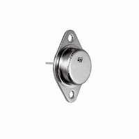
... Fast switching speed Applications ■ High frequency and efficency converters ■ Linear and switching industrial equipment Description The BUX98A is a multi-epitaxial mesa NPN transistor in TO-3 metal case, intended for industrial applications from single and three- phase mains operation. Table 1. Device summary Order codes ...
Page 2
... Content Content 1 Electrical ratings . . . . . . . . . . . . . . . . . . . . . . . . . . . . . . . . . . . . . . . . . . . . 3 2 Electrical characteristics . . . . . . . . . . . . . . . . . . . . . . . . . . . . . . . . . . . . . 4 2.1 Electrical characteristics (curves Test circuits . . . . . . . . . . . . . . . . . . . . . . . . . . . . . . . . . . . . . . . . . . . . . . . . 7 4 Package mechanical data . . . . . . . . . . . . . . . . . . . . . . . . . . . . . . . . . . . . . 8 5 Revision history . . . . . . . . . . . . . . . . . . . . . . . . . . . . . . . . . . . . . . . . . . . 10 2/11 BUX98A ...
Page 3
... BUX98A 1 Electrical ratings Table 2. Absolute maximum ratings Symbol V Collector-emitter voltage (R CER V Collector-emitter voltage (V CES V Collector-emitter voltage (I CEO V Emitter-base voltage (I EBO I Collector current C I Collector peak current ( Collector peak current non repetitive ( Base current B I Base peak current ( Total power dissipation at T TOT ...
Page 4
... Pulsed duration = 300 µs, duty cycle ≤ 1.5% 4/11 Parameter Test conditions V = 1000 1000 1000 Ω 1000 1000 200 Ω B(on) B(off) Min. Typ. Max. 400 = 125 ° 125 ° 450 1000 I = 3 3 150 3.2 A 0.8 BUX98A Unit µA mA µA µ µs µs µs ...
Page 5
... BUX98A 2.1 Electrical characteristics (curves) Figure 2. Safe operating area Figure 4. DC current gain ° 0.1 1 Figure 6. Base-emitter saturation voltage V BE(sat °C j 0.5 0 0.1 1 Figure 3. Figure 5. AM03275v1 V CE(sat 125 ° (A) C Figure 7. AM03277v1 T = 125 ° (A) C Electrical characteristics Derating curve Collector-emitter saturation voltage ...
Page 6
... Electrical characteristics Figure 8. Resistive load switching times (off) Figure 9. t (µ 150 V, V BE(off B(on B(off Fall time 0 6/11 AM03279v1 I C Storage time 25 I (A) C Reverse biased SOA (A) V BE(off BE(off 100 µ 100 1000 V CE BUX98A AM03280v1 (V) ...
Page 7
... BUX98A 3 Test circuits Figure 10. Resistive load switching test circuit 1) Fast electronic switch 2) Non-inductive resistor Test circuits 7/11 ...
Page 8
... These packages have a lead-free second level interconnect . The category of second level interconnect is marked on the package and on the inner box label, in compliance with JEDEC Standard JESD97. The maximum ratings related to soldering conditions are also marked on the inner box label. ECOPACK trademark. ECOPACK specifications are available at: www.st.com 8/11 BUX98A ...
Page 9
... BUX98A DIM TO-3 type R Mechanical data m m MIN. TYP. MAX Package mechanical data MIN. TYP. MAX 0015929_C 9/11 ...
Page 10
... Revision history 5 Revision history Table 5. Document revision history Date 21-Jun-2004 24-Nov-2008 10/11 Revision 4 Section 2.1: Electrical characteristics (curves) 5 Inserted new BUX98A Changes ...
Page 11
... BUX98A Information in this document is provided solely in connection with ST products. STMicroelectronics NV and its subsidiaries (“ST”) reserve the right to make changes, corrections, modifications or improvements, to this document, and the products and services described herein at any time, without notice. All ST products are sold pursuant to ST’s terms and conditions of sale. ...