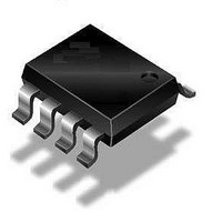
ATA6620N-TASY Atmel, ATA6620N-TASY Datasheet - Page 13

ATA6620N-TASY
Manufacturer Part Number
ATA6620N-TASY
Description
RF Wireless Misc LIN SBC
Manufacturer
Atmel
Datasheet
1.ATA6620N-TAQY.pdf
(22 pages)
Specifications of ATA6620N-TASY
Package / Case
SOIC
Mounting Style
SMD/SMT
Lead Free Status / RoHS Status
Lead free / RoHS Compliant
7. Absolute Maximum Ratings
Stresses beyond those listed under “Absolute Maximum Ratings” may cause permanent damage to the device. This is a stress rating
only and functional operation of the device at these or any other conditions beyond those indicated in the operational sections of this
specification is not implied. Exposure to absolute maximum rating conditions for extended periods may affect device reliability.
4850I–AUTO–09/09
Parameters
Supply voltage V
Pulse time 500 ms
T = 25°C
Output current I
Pulse time 2 min
T = 25°C
Output current I
Logic pins (RXD, TXD, EN, NRES)
Output current NRES
LIN
- DC voltage
- Transient voltage
V
- DC voltage
ESD (DIN EN 6100–4–2)
Pin LIN, V
specification EMC Evaluation V 1.3
HBM ESD S5.1 – all pins
CDM ESD STM 5.3.1–1999
- All pins
Junction temperature
Storage temperature
Operating ambient temperature
Thermal resistance junction to ambient
(free air)
Special heat sink at GND (pin 3) on PCB
Thermal shutdown of V
Thermal shutdown of LIN output
Thermal shutdown hysteresis
CC
S
versus GND according to LIN
VCC
VCC
S
50 mA
50 mA
CC
regulator
Symbol
T
T
I
R
R
NRES
VCCoff
T
LINoff
V
V
V
T
T
T
thja
thja
hys
a
S
S
S
s
j
–1000
–150
Min.
–0.3
–0.3
–0.3
–40
–40
–55
–40
150
150
–2
–6
–3
Typ.
160
160
80
10
+1000
Max.
+100
+150
+150
+125
+6.5
+6.5
+40
+40
+60
145
170
170
27
+2
+6
+3
ATA6620N
Unit
K/W
K/W
mA
kV
kV
°C
°C
°C
°C
°C
°C
V
V
V
V
V
V
V
V
13


