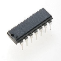
MC1496P ON Semiconductor, MC1496P Datasheet - Page 8

MC1496P
Manufacturer Part Number
MC1496P
Description
Modulator / Demodulator Balanced Mod/DeMod
Manufacturer
ON Semiconductor
Datasheet
1.MC1496DR2G.pdf
(14 pages)
Specifications of MC1496P
Package / Case
PDIP-14
Maximum Operating Temperature
+ 70 C
Maximum Power Dissipation
33 mW
Minimum Operating Temperature
0 C
Modulation Type
Balanced
Mounting Style
Through Hole
Supply Current
0.005 A
Lead Free Status / RoHS Status
Lead free / RoHS Compliant
Available stocks
Company
Part Number
Manufacturer
Quantity
Price
Company:
Part Number:
MC1496P
Manufacturer:
MOTOROLA
Quantity:
8
Part Number:
MC1496P
Manufacturer:
ON/安森美
Quantity:
20 000
Part Number:
MC1496PG
Manufacturer:
ON/安森美
Quantity:
20 000
shown in Figure 23.
driven by a standard differential amplifier with dual current
sources. The output collectors are cross−coupled so that
full−wave balanced multiplication of the two input voltages
occurs. That is, the output signal is a constant times the
product of the two input signals.
indicates that the output spectrum will consist of only the sum
and difference of the two input frequencies. Thus, the device
may be used as a balanced modulator, doubly balanced mixer,
product detector, frequency doubler, and other applications
requiring these particular output signal characteristics.
to the package pins so that an external emitter resistance may
be used. Also, external load resistors are employed at the
device output.
Signal Levels
either in a linear or a saturated mode. The lower differential
amplifier is operated in a linear mode for most applications.
signal will contain sum and difference frequency
Carrier
Signal
The MC1496, a monolithic balanced modulator circuit, is
This circuit consists of an upper quad differential amplifier
Mathematical analysis of linear ac signal multiplication
The lower differential amplifier has its emitters connected
The upper quad differential amplifier may be operated
For low−level operation at both input ports, the output
Input
Input
Bias
V
10
20
30
40
50
60
70
0.05
EE
0
V
V
14
5
C
S
10 (−)
Figure 21. Suppression of Carrier Harmonic
8 (+)
4 (−)
1 (+)
500
0.1
Sidebands versus Carrier Frequency
Figure 23. Circuit Schematic
500
f
C
, CARRIER FREQUENCY (MHz)
0.5
1.0
2f
2f
3f
C
C
500
5.0
C
± 2f
± f
± f
S
S
OPERATIONS INFORMATION
S
(−) 12
(Pin numbers
per G package)
(+) 6
10
2
3
V
Output
Gain
Adjust
http://onsemi.com
o
,
50
8
Modulating
Carrier
Input
components and have an amplitude which is a function of the
product of the input signal amplitudes.
linear operation at the modulating signal port, the output
signal will contain sum and difference frequency
components of the modulating signal frequency and the
fundamental and odd harmonics of the carrier frequency.
The output amplitude will be a constant times the
modulating signal amplitude. Any amplitude variations in
the carrier signal will not appear in the output.
amplifier are well defined. With no emitter degeneration, the
maximum
approximately 25 mV peak. Since the upper differential
amplifier has its emitters internally connected, this voltage
applies to the carrier input port for all conditions.
external emitter resistance, its linear signal handling range
may be adjusted by the user. The maximum input voltage for
linear operation may be approximated from the following
expression:
value of R
Signal
Input
For high−level operation at the carrier input port and
The linear signal handling capabilities of a differential
Since the lower differential amplifier has provisions for an
This expression may be used to compute the minimum
10
20
30
40
50
60
70
V
V
0
C
S
0
0.1 mF
10 k
1.0 k
E
Carrier Null
Figure 24. Typical Modulator Circuit
Figure 22. Carrier Suppression versus
for a given input voltage amplitude.
input
50 k
10 k
51
100
V = (I5) (R
V
C
, CARRIER INPUT LEVEL (mVrms)
voltage
51
Carrier Input Level
0.1 mF
200
51
1.0 k
E
10
8
1
4
) volts peak.
for
2
V
EE
MC1496
14
−8.0 Vdc
300
R
e
linear
1.0 k
f
f
C
C
I5
= 500 kHz
= 10 MHz
3
5
6.8 k
operation
400
3.9 k
12
6
R
L
12 Vdc
3.9 k
R
500
−V
+V
L
is
o
o


