MJE13003G ON Semiconductor, MJE13003G Datasheet

TRANS POWER NPN 1.5A 400V TO-225

MJE13003G

Manufacturer Part Number
MJE13003G
Description
TRANS POWER NPN 1.5A 400V TO-225
Manufacturer
ON Semiconductor
Series
SWITCHMODE™r
Datasheet

Specifications of MJE13003G

Transistor Type
NPN
Current - Collector (ic) (max)
1.5A
Voltage - Collector Emitter Breakdown (max)
400V
Vce Saturation (max) @ Ib, Ic
3V @ 500mA, 1.5A
Dc Current Gain (hfe) (min) @ Ic, Vce
8 @ 500mA, 2V
Power - Max
1.4W
Frequency - Transition
10MHz
Mounting Type
Through Hole
Package / Case
TO-225-3
Lead Free Status / RoHS Status
Lead free / RoHS Compliant
Current - Collector Cutoff (max)
-
Other names
MJE13003G
MJE13003GOS
Î Î Î Î Î Î Î Î Î Î Î Î
MJE13003
SWITCHMODEt Series NPN
Silicon Power Transistor
switching inductive circuits where fall time is critical. They are
particularly suited for 115 and 220 V SWITCHMODE applications
such as Switching Regulators, Inverters, Motor Controls,
Solenoid/Relay drivers and Deflection circuits.
Features
Maximum ratings are those values beyond which device damage can occur.
Maximum ratings applied to the device are individual stress limit values (not
normal operating conditions) and are not valid simultaneously. If these limits are
exceeded, device functional operation is not implied, damage may occur and
reliability may be affected.
1. Pulse Test: Pulse Width = 5 ms, Duty Cycle ≤ 10%.
*For additional information on our Pb−Free strategy and soldering details, please
© Semiconductor Components Industries, LLC, 2006
January, 2006 − Rev. 2
MAXIMUM RATINGS
THERMAL CHARACTERISTICS
download the ON Semiconductor Soldering and Mounting Techniques
Reference Manual, SOLDERRM/D.
Collector−Emitter Voltage
Emitter Base Voltage
Collector Current
Base Current
Emitter Current
Total Power Dissipation @ T
Operating and Storage Junction
Thermal Resistance, Junction−to−Case
Thermal Resistance, Junction−to−Ambient
Maximum Load Temperature for Soldering
Purposes: 1/8″ from Case for 5 Seconds
These devices are designed for high−voltage, high−speed power
Reverse Biased SOA with Inductive Loads @ T
Inductive Switching Matrix 0.5 to 1.5 A, 25 and 100_C
700 V Blocking Capability
SOA and Switching Applications Information
Pb−Free Package is Available*
Derate above 25_C
Derate above 25_C
Temperature Range
t
c
Characteristic
@ 1 A, 100_C is 290 ns (Typ)
Rating
− Continuous
− Continuous
− Continuous
− Peak (Note 1)
− Peak (Note 1)
− Peak (Note 1)
A
C
= 25_C
= 25_C
Î Î Î
Î Î Î
Î Î Î
Î Î Î
Î Î Î
Î Î Î
Î Î Î
Î Î Î
Î Î Î
Î Î Î
Î Î Î
Î Î Î
Î Î Î
Î Î Î
Î Î Î
Î Î Î
Î Î Î
Î Î Î
Î Î Î
Î Î Î
Î Î Î
Î Î Î
Î Î Î
Î Î Î
Î Î Î
Î Î Î
Î Î Î
V
Symbol
Symbol
T
CEO(sus)
V
V
R
R
J
I
I
I
P
P
, T
EBO
T
CEV
I
CM
BM
EM
I
I
qJC
qJA
C
B
E
D
D
L
stg
Î Î Î Î
Î Î Î Î
Î Î Î Î
Î Î Î Î
Î Î Î Î
Î Î Î Î
Î Î Î Î
Î Î Î Î
Î Î Î Î
Î Î Î Î
Î Î Î Î
Î Î Î Î
Î Î Î Î
Î Î Î Î
Î Î Î Î
Î Î Î Î
Î Î Î Î
Î Î Î Î
Î Î Î Î
Î Î Î Î
Î Î Î Î
Î Î Î Î
Î Î Î Î
Î Î Î Î
Î Î Î Î
Î Î Î Î
Î Î Î Î
C
Value
–65 to
= 100_C
+150
0.75
2.25
11.2
Max
3.12
400
700
320
275
1.5
1.5
4.5
1.4
40
89
9
3
Î Î Î
Î Î Î
Î Î Î
Î Î Î
Î Î Î
Î Î Î
Î Î Î
Î Î Î
Î Î Î
Î Î Î
Î Î Î
Î Î Î
Î Î Î
Î Î Î
Î Î Î
Î Î Î
Î Î Î
Î Î Î
Î Î Î
Î Î Î
Î Î Î
Î Î Î
Î Î Î
Î Î Î
Î Î Î
Î Î Î
Î Î Î
1
mW/_C
mW/_C
_C/W
_C/W
Unit
Unit
Vdc
Vdc
Vdc
Adc
Adc
Adc
_C
_C
W
W
MJE13003
MJE13003G
Device
2 COLLECTOR
NPN SILICON POWER
3
300 AND 400 VOLTS
ORDERING INFORMATION
3 EMITTER
Y
WW
JE13003
G
2 1
1 BASE
MARKING DIAGRAM
TRANSISTORS
1.5 AMPERES
http://onsemi.com
40 WATTS
(Pb−Free)
Package
TO−225
TO−225
= Year
= Work Week
= Device Code
= Pb−Free Package
Publication Order Number:
CASE 77
STYLE 3
TO−225
13003G
YWW
500 Units/Box
500 Units/Box
JE
Shipping
MJE13003/D

Related parts for MJE13003G

MJE13003G Summary of contents

Page 1

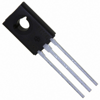
... AND 400 VOLTS 40 WATTS TO−225 CASE 77 STYLE MARKING DIAGRAM 1 BASE YWW 2 COLLECTOR JE 13003G 3 EMITTER Y = Year WW = Work Week JE13003 = Device Code G = Pb−Free Package ORDERING INFORMATION Device Package Shipping MJE13003 TO−225 500 Units/Box TO−225 500 Units/Box MJE13003G (Pb−Free) Publication Order Number: MJE13003/D ...

Page 2

ELECTRICAL CHARACTERISTICS Î Î Î Î Î ...

Page 3

T = 150° 25°C 20 −55 ° 0.02 0.05 0.07 0.1 0.2 0.3 0. COLLECTOR CURRENT (AMP) C Figure ...

Page 4

Table 1. Test Conditions for Dynamic Performance REVERSE BIAS SAFE OPERATING AREA AND INDUCTIVE SWITCHING 1N4933 0.001 2N222 DUTY CYCLE ≤ 10% 68 ≤ ...

Page 5

I CPK 90% V clamp 10 clamp I 90 TIME Figure 7. Inductive Switching Measurements NOTE: All Data Recorded in the Inductive Switching Circuit in Table 1 In ...

Page 6

RESISTIVE SWITCHING PERFORMANCE 125 0 25° 0.5 0.3 0 BE(off) 0.1 0.07 0.05 0.03 0.02 0.02 ...

Page 7

The Safe Operating Area figures shown in Figures 11 and 12 are specified ratings for these devices under the test conditions shown 5 0 25°C C 0.2 THERMAL LIMIT (SINGLE PULSE) 0.1 ...

Page 8

... American Technical Support: 800−282−9855 Toll Free USA/Canada Japan: ON Semiconductor, Japan Customer Focus Center 2−9−1 Kamimeguro, Meguro−ku, Tokyo, Japan 153−0051 Phone: 81−3−5773−3850 http://onsemi.com 8 NOTES: 1. DIMENSIONING AND TOLERANCING PER ANSI Y14.5M, 1982. 2. CONTROLLING DIMENSION: INCH. ...

Related keywords