BC847CTT1 ON Semiconductor, BC847CTT1 Datasheet

TRANS NPN GP 45V 100MA SC75-3

BC847CTT1

Manufacturer Part Number
BC847CTT1
Description
TRANS NPN GP 45V 100MA SC75-3
Manufacturer
ON Semiconductor
Datasheet

Specifications of BC847CTT1

Transistor Type
NPN
Current - Collector (ic) (max)
100mA
Voltage - Collector Emitter Breakdown (max)
45V
Vce Saturation (max) @ Ib, Ic
600mV @ 5mA, 100mA
Dc Current Gain (hfe) (min) @ Ic, Vce
420 @ 2mA, 5V
Power - Max
225mW
Frequency - Transition
100MHz
Mounting Type
Surface Mount
Package / Case
SC-75-3, SOT-416, EMT3, 3-SSMini
Lead Free Status / RoHS Status
Contains lead / RoHS non-compliant
Current - Collector Cutoff (max)
-

Available stocks

Company
Part Number
Manufacturer
Quantity
Price
Part Number:
BC847CTT1
Manufacturer:
ON/安森美
Quantity:
20 000
Part Number:
BC847CTT1G
Manufacturer:
ON Semiconductor
Quantity:
28 038
Part Number:
BC847CTT1G
Manufacturer:
ON Semiconductor
Quantity:
1 800
Part Number:
BC847CTT1G
Manufacturer:
ON
Quantity:
30 000
BC847ATT1, BC847BTT1,
BC847CTT1
General Purpose
Transistors
NPN Silicon
applications. They are housed in the SC−75/SOT−416 package which
is designed for low power surface mount applications.
Features
1. FR−4 @ min pad.
2. FR−4 @ 1.0
*For additional information on our Pb−Free strategy and soldering details, please
MAXIMUM RATINGS
THERMAL CHARACTERISTICS
June, 2004 − Rev. 1
Maximum ratings are those values beyond which device damage can occur.
Maximum ratings applied to the device are individual stress limit values (not
normal operating conditions) and are not valid simultaneously. If these limits
are exceeded, device functional operation is not implied, damage may occur
and reliability may be affected.
download the ON Semiconductor Soldering and Mounting Techniques
Reference Manual, SOLDERRM/D.
Collector−Emitter Voltage
Collector−Base Voltage
Emitter−Base Voltage
Collector Current − Continuous
Total Device Dissipation,
Thermal Resistance,
Total Device Dissipation,
Thermal Resistance,
Junction and Storage
These transistors are designed for general purpose amplifier
Pb−Free Packages are Available*
Semiconductor Components Industries, LLC, 2004
FR−4 Board (Note 1)
T
Derated above 25 C
Junction−to−Ambient (Note 1)
FR−4 Board (Note 2)
T
Derated above 25 C
Junction−to−Ambient (Note 2)
Temperature Range
A
A
= 25 C
= 25 C
Characteristic
1.0 in pad.
Rating
(T
A
= 25 C)
Symbol
Symbol
T
V
V
V
R
R
J
P
P
CEO
CBO
EBO
, T
I
qJA
qJA
C
D
D
stg
−55 to
+150
Max
Max
100
200
600
300
400
6.0
1.6
2.4
45
50
1
mW/ C
mW/ C
mAdc
Unit
Unit
mW
mW
C/W
C/W
V
V
V
C
See detailed ordering and shipping information in the package
dimensions section on page 5 of this data sheet.
ORDERING INFORMATION
3
MARKING DIAGRAM
1
BASE
http://onsemi.com
1
xx = Device Code
M = Date Code
2
COLLECTOR
EMITTER
xxM
SC−75/SOT−41
Publication Order Number:
3
2
CASE 463
STYLE 1
6
BC847ATT1/D

Related parts for BC847CTT1

BC847CTT1 Summary of contents

Page 1

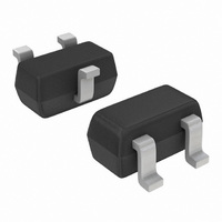
... BC847ATT1, BC847BTT1, BC847CTT1 General Purpose Transistors NPN Silicon These transistors are designed for general purpose amplifier applications. They are housed in the SC−75/SOT−416 package which is designed for low power surface mount applications. Features Pb−Free Packages are Available* MAXIMUM RATINGS ( Rating Collector−Emitter Voltage Collector− ...

Page 2

... BC847ATT1, BC847BTT1, BC847CTT1 ELECTRICAL CHARACTERISTICS Characteristic OFF CHARACTERISTICS Collector −Emitter Breakdown Voltage ( mA) C Collector −Emitter Breakdown Voltage = 10 mA Collector −Base Breakdown Voltage = 10 mA Emitter −Base Breakdown Voltage = 1.0 mA Collector Cutoff Current ( CHARACTERISTICS DC Current Gain = 2 Collector −Emitter Saturation Voltage (I C Collector − ...

Page 3

... BC847ATT1, BC847BTT1, BC847CTT1 2.0 1.5 1.0 0.8 0.6 0.4 0.3 0.2 0.2 0.5 1.0 2.0 5 COLLECTOR CURRENT (mAdc) C Figure 1. Normalized DC Current Gain 2 1.6 1 0.8 0.4 0 0.02 0.1 1 BASE CURRENT (mA) B Figure 3. Collector Saturation Region 1 0 0.8 0.7 0.6 0.5 0.4 0.3 ...

Page 4

... BC847ATT1, BC847BTT1, BC847CTT1 1 0.5 0.2 0.1 0.1 0.05 0.02 0.01 0.01 SINGLE PULSE 0.001 0.00001 0.0001 0.001 Figure 5. Normalized Thermal Response 10 7 2.0 1.0 0.4 0.6 0.8 1.0 2.0 4.0 6.0 8 REVERSE VOLTAGE (VOLTS) R Figure 6. Capacitances BC847 0.01 0.1 t, TIME (s) ...

Page 5

... BC847ATT1, BC847BTT1, BC847CTT1 ORDERING INFORMATION Device BC847ATT1 BC847BTT1 BC847BTT1G BC847CTT1 BC847CTT1G †For information on tape and reel specifications, including part orientation and tape sizes, please refer to our Tape and Reel Packaging Specifi- cations Brochure, BRD8011/D. Marking Package 1E SC−75/SOT−416 1F SC−75/SOT−416 1F SC− ...

Page 6

... BC847ATT1, BC847BTT1, BC847CTT1 −A− 0.20 (0.008 Semiconductor and are registered trademarks of Semiconductor Components Industries, LLC (SCILLC). SCILLC reserves the right to make changes without further notice to any products herein. SCILLC makes no warranty, representation or guarantee regarding the suitability of its products for any particular purpose, nor does SCILLC assume any liability arising out of the application or use of any product or circuit, and specifically disclaims any and all liability, including without limitation special, consequential or incidental damages. “ ...

Related keywords