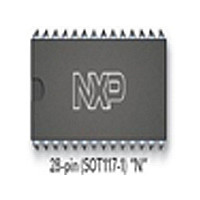
SJA1000 NXP Semiconductors, SJA1000 Datasheet - Page 53

SJA1000
Manufacturer Part Number
SJA1000
Description
Manufacturer
NXP Semiconductors
Datasheet
1.SJA1000.pdf
(68 pages)
Specifications of SJA1000
Data Rate
1000Kbps
Number Of Transceivers
1
Power Down Mode
Sleep
Standard Supported
CAN 2.0B
Operating Supply Voltage (max)
5.5V
Operating Supply Voltage (typ)
5V
Operating Supply Voltage (min)
4.5V
Package Type
PDIP
Supply Current
15mA
Operating Temperature (max)
125C
Operating Temperature (min)
-40C
Operating Temperature Classification
Automotive
Mounting
Through Hole
Pin Count
28
Lead Free Status / RoHS Status
Compliant
Available stocks
Company
Part Number
Manufacturer
Quantity
Price
Part Number:
SJA1000
Manufacturer:
PHILIPS/飞利浦
Quantity:
20 000
Company:
Part Number:
SJA1000N
Manufacturer:
NXP
Quantity:
5 510
Part Number:
SJA1000N
Manufacturer:
PHILIPS/飞利浦
Quantity:
20 000
Part Number:
SJA1000T
Manufacturer:
NXP
Quantity:
20 000
Part Number:
SJA1000T SJ
Manufacturer:
NXP/恩智浦
Quantity:
20 000
Part Number:
SJA1000T/N1
Manufacturer:
NXP/恩智浦
Quantity:
20 000
Company:
Part Number:
SJA1000T/N1,118
Manufacturer:
XILINX
Quantity:
125
Philips Semiconductors
6.5.3.2
For the TX0 pin this is the same as in normal output mode. However, the data stream to TX1 is replaced by the transmit
clock (TXCLK). The rising edge of the transmit clock (non-inverted) marks the beginning of a bit period. The clock pulse
width is 1
6.5.3.3
In contrast to the normal output mode the bit
representation is time variant and toggled. If the bus
controllers are galvanically decoupled from the bus line by
a transformer, the bit stream is not allowed to contain a
DC component. This is achieved by the following scheme.
2000 Jan 04
handbook, full pagewidth
Stand-alone CAN controller
Clock output mode
Bi-phase output mode
t
scl
.
TX0
TX1
HIGH
HIGH
LOW
LOW
1 bit time
Fig.15 Example of clock output mode.
53
During recessive bits all outputs are deactivated (floating).
Dominant bits are sent with alternating levels on TX0 and
TX1, i.e. the first dominant bit is sent on TX0, the second
is sent on TX1, and the third one is sent on TX0 again, and
so on. One possible configuration example of the bi-phase
output mode timing is shown in Fig.16.
MGK630
Product specification
SJA1000


