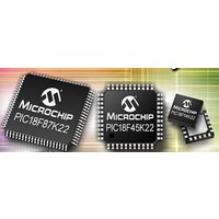
PIC18F46K22-I/MV Microchip Technology, PIC18F46K22-I/MV Datasheet - Page 165

PIC18F46K22-I/MV
Manufacturer Part Number
PIC18F46K22-I/MV
Description
64KB, Flash, 3968bytes-RAM,8-bit Family,nanoWatt XLP 40 UQFN 5x5x0.5mm TUBE
Manufacturer
Microchip Technology
Series
PIC® XLP™ 18Fr
Datasheet
1.PIC18F26J13-ISS.pdf
(496 pages)
Specifications of PIC18F46K22-I/MV
Core Processor
PIC
Core Size
8-Bit
Speed
64MHz
Connectivity
I²C, SPI, UART/USART
Peripherals
Brown-out Detect/Reset, HLVD, POR, PWM, WDT
Number Of I /o
35
Program Memory Size
64KB (32K x 16)
Program Memory Type
FLASH
Eeprom Size
1K x 8
Ram Size
3.8K x 8
Voltage - Supply (vcc/vdd)
1.8 V ~ 5.5 V
Data Converters
A/D 30x10b
Oscillator Type
Internal
Operating Temperature
-40°C ~ 85°C
Package / Case
40-UFQFN Exposed Pad
Processor Series
PIC18F
Core
PIC
Data Bus Width
8 bit
Data Ram Size
4 KB
Number Of Programmable I/os
36
Number Of Timers
3 x 8-bit. 4 x 16-bit
Operating Supply Voltage
1.8 V to 5.5 V
Mounting Style
SMD/SMT
Lead Free Status / RoHS Status
Lead free / RoHS Compliant
Lead Free Status / RoHS Status
Lead free / RoHS Compliant
- Current page: 165 of 496
- Download datasheet (5Mb)
12.7.2.3
The output resulting from a Comparator 1 operation can
be selected as a source for Timer1/3/5 Gate Control.
The Comparator 1 output (SYNCC1OUT) can be
synchronized
asynchronous. For more information see Section 18.8.4
“Synchronizing Comparator Output to Timer1”.
12.7.2.4
The output resulting from a Comparator 2 operation
can be selected as a source for Timer1/3/5 Gate
Control. The Comparator 2 output (SYNCC2OUT) can
be synchronized to the Timer1/3/5 clock or left
asynchronous.
Section 18.8.4 “Synchronizing Comparator Output
to Timer1”.
12.7.3
When Timer1/3/5 Gate Toggle mode is enabled, it is
possible to measure the full-cycle length of a
Timer1/3/5 gate signal, as opposed to the duration of a
single level pulse.
The Timer1/3/5 Gate source is routed through a
flip-flop that changes state on every incrementing edge
of the signal. See
Timer1/3/5 Gate Toggle mode is enabled by setting the
TxGTM bit of the TxGCON register. When the TxGTM
bit is cleared, the flip-flop is cleared and held clear. This
is necessary in order to control which edge is
measured.
2010 Microchip Technology Inc.
Note:
TIMER1/3/5 GATE TOGGLE MODE
Enabling Toggle mode at the same time
as changing the gate polarity may result in
indeterminate operation.
Comparator C1 Gate Operation
Comparator C2 Gate Operation
to
Figure 12-5
For
the
Timer1/3/5
more
for timing details.
information
clock
or
see
Preliminary
left
12.7.4
When Timer1/3/5 Gate Single-Pulse mode is enabled,
it is possible to capture a single-pulse gate event.
Timer1/3/5 Gate Single-Pulse mode is first enabled by
setting the TxGSPM bit in the TxGCON register. Next,
the TxGGO/DONE bit in the TxGCON register must be
set. The Timer1/3/5 will be fully enabled on the next
incrementing edge. On the next trailing edge of the
pulse, the TxGGO/DONE bit will automatically be
cleared. No other gate events will be allowed to
increment Timer1/3/5 until the TxGGO/DONE bit is
once again set in software.
Clearing the TxGSPM bit of the TxGCON register will
also clear the TxGGO/DONE bit. See
timing details.
Enabling the Toggle mode and the Single-Pulse mode
simultaneously will permit both sections to work
together. This allows the cycle times on the Timer1/3/5
Gate source to be measured. See
timing details.
12.7.5
When Timer1/3/5 Gate Value Status is utilized, it is
possible to read the most current level of the gate
control value. The value is stored in the TxGVAL bit in
the TxGCON register. The TxGVAL bit is valid even
when the Timer1/3/5 Gate is not enabled (TMRxGE bit
is cleared).
12.7.6
When Timer1/3/5 Gate Event Interrupt is enabled, it is
possible to generate an interrupt upon the completion
of a gate event. When the falling edge of TxGVAL
occurs, the TMRxGIF flag bit in the PIR3 register will be
set. If the TMRxGIE bit in the PIE3 register is set, then
an interrupt will be recognized.
The TMRxGIF flag bit operates even when the
Timer1/3/5 Gate is not enabled (TMRxGE bit is
cleared).
For more information on selecting high or low priority
status for the Timer1/3/5 Gate Event Interrupt see
Section 9.0
PIC18(L)F2X/4XK22
TIMER1/3/5 GATE SINGLE-PULSE
MODE
TIMER1/3/5 GATE VALUE STATUS
TIMER1/3/5 GATE EVENT
INTERRUPT
“Interrupts”.
DS41412D-page 165
Figure 12-7
Figure 12-6
for
for
Related parts for PIC18F46K22-I/MV
Image
Part Number
Description
Manufacturer
Datasheet
Request
R

Part Number:
Description:
Manufacturer:
Microchip Technology Inc.
Datasheet:

Part Number:
Description:
Manufacturer:
Microchip Technology Inc.
Datasheet:

Part Number:
Description:
Manufacturer:
Microchip Technology Inc.
Datasheet:

Part Number:
Description:
Manufacturer:
Microchip Technology Inc.
Datasheet:

Part Number:
Description:
Manufacturer:
Microchip Technology Inc.
Datasheet:

Part Number:
Description:
Manufacturer:
Microchip Technology Inc.
Datasheet:

Part Number:
Description:
Manufacturer:
Microchip Technology Inc.
Datasheet:

Part Number:
Description:
Manufacturer:
Microchip Technology Inc.
Datasheet:


