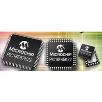
PIC18F46K22-I/MV Microchip Technology, PIC18F46K22-I/MV Datasheet - Page 211

PIC18F46K22-I/MV
Manufacturer Part Number
PIC18F46K22-I/MV
Description
64KB, Flash, 3968bytes-RAM,8-bit Family,nanoWatt XLP 40 UQFN 5x5x0.5mm TUBE
Manufacturer
Microchip Technology
Series
PIC® XLP™ 18Fr
Datasheet
1.PIC18F26J13-ISS.pdf
(496 pages)
Specifications of PIC18F46K22-I/MV
Core Processor
PIC
Core Size
8-Bit
Speed
64MHz
Connectivity
I²C, SPI, UART/USART
Peripherals
Brown-out Detect/Reset, HLVD, POR, PWM, WDT
Number Of I /o
35
Program Memory Size
64KB (32K x 16)
Program Memory Type
FLASH
Eeprom Size
1K x 8
Ram Size
3.8K x 8
Voltage - Supply (vcc/vdd)
1.8 V ~ 5.5 V
Data Converters
A/D 30x10b
Oscillator Type
Internal
Operating Temperature
-40°C ~ 85°C
Package / Case
40-UFQFN Exposed Pad
Processor Series
PIC18F
Core
PIC
Data Bus Width
8 bit
Data Ram Size
4 KB
Number Of Programmable I/os
36
Number Of Timers
3 x 8-bit. 4 x 16-bit
Operating Supply Voltage
1.8 V to 5.5 V
Mounting Style
SMD/SMT
Lead Free Status / RoHS Status
Lead free / RoHS Compliant
Lead Free Status / RoHS Status
Lead free / RoHS Compliant
- Current page: 211 of 496
- Download datasheet (5Mb)
FIGURE 15-4:
15.2.1 SPI MODE REGISTERS
The MSSPx module has five registers for SPI mode
operation. These are:
• MSSPx STATUS register (SSPxSTAT)
• MSSPx Control register 1 (SSPxCON1)
• MSSPx Control register 3 (SSPxCON3)
• MSSPx Data Buffer register (SSPxBUF)
• MSSPx Address register (SSPxADD)
• MSSPx Shift register (SSPxSR)
SSPxCON1 and SSPxSTAT are the control and
STATUS registers in SPI mode operation. The
SSPxCON1 register is readable and writable. The
lower 6 bits of the SSPxSTAT are read-only. The
upper two bits of the SSPxSTAT are read/write.
In one SPI Master mode, SSPxADD can be loaded
with a value used in the Baud Rate Generator. More
information on the Baud Rate Generator is available in
Section 15.7 “Baud Rate
SSPxSR is the shift register used for shifting data in
and out. SSPxBUF provides indirect access to the
SSPxSR register. SSPxBUF is the buffer register to
which data bytes are written, and from which data
bytes are read.
In receive operations, SSPxSR and SSPxBUF
together create a buffered receiver. When SSPxSR
receives a complete byte, it is transferred to SSPxBUF
and the SSPxIF interrupt is set.
During transmission, the SSPxBUF is not buffered. A
write to SSPxBUF will write to both SSPxBUF and
SSPxSR.
2010 Microchip Technology Inc.
(Not directly accessible)
SPI Master
SPI MASTER AND MULTIPLE SLAVE CONNECTION
Generator”.
General I/O
General I/O
General I/O
SDOx
SCLK
SDIx
Preliminary
15.2.2 SPI MODE OPERATION
When initializing the SPI, several options need to be
specified. This is done by programming the appropriate
control bits (SSPxCON1<5:0> and SSPxSTAT<7:6>).
These control bits allow the following to be specified:
• Master mode (SCKx is the clock output)
• Slave mode (SCKx is the clock input)
• Clock Polarity (Idle state of SCKx)
• Data Input Sample Phase (middle or end of data
• Clock Edge (output data on rising/falling edge of
• Clock Rate (Master mode only)
• Slave Select mode (Slave mode only)
To enable the serial port, SSPx Enable bit, SSPxEN of
the SSPxCON1 register, must be set. To reset or
reconfigure SPI mode, clear the SSPxEN bit, re-initial-
ize the SSPxCONx registers and then set the SSPxEN
bit. This configures the SDIx, SDOx, SCKx and SSx
pins as serial port pins. For the pins to behave as the
serial port function, some must have their data direction
bits (in the TRIS register) appropriately programmed as
follows:
• SDIx must have corresponding TRIS bit set
• SDOx must have corresponding TRIS bit cleared
• SCKx (Master mode) must have corresponding
• SCKx (Slave mode) must have corresponding
• SSx must have corresponding TRIS bit set
output time)
SCKx)
TRIS bit cleared
TRIS bit set
PIC18(L)F2X/4XK22
SCLK
SDIx
SDOx
SSx
SCLK
SDIx
SDOx
SSx
SCLK
SDIx
SDOx
SSx
SPI Slave
SPI Slave
SPI Slave
#1
#2
#3
DS41412D-page 211
Related parts for PIC18F46K22-I/MV
Image
Part Number
Description
Manufacturer
Datasheet
Request
R

Part Number:
Description:
Manufacturer:
Microchip Technology Inc.
Datasheet:

Part Number:
Description:
Manufacturer:
Microchip Technology Inc.
Datasheet:

Part Number:
Description:
Manufacturer:
Microchip Technology Inc.
Datasheet:

Part Number:
Description:
Manufacturer:
Microchip Technology Inc.
Datasheet:

Part Number:
Description:
Manufacturer:
Microchip Technology Inc.
Datasheet:

Part Number:
Description:
Manufacturer:
Microchip Technology Inc.
Datasheet:

Part Number:
Description:
Manufacturer:
Microchip Technology Inc.
Datasheet:

Part Number:
Description:
Manufacturer:
Microchip Technology Inc.
Datasheet:


