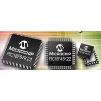
PIC18F46K22-I/MV Microchip Technology, PIC18F46K22-I/MV Datasheet - Page 259

PIC18F46K22-I/MV
Manufacturer Part Number
PIC18F46K22-I/MV
Description
64KB, Flash, 3968bytes-RAM,8-bit Family,nanoWatt XLP 40 UQFN 5x5x0.5mm TUBE
Manufacturer
Microchip Technology
Series
PIC® XLP™ 18Fr
Datasheet
1.PIC18F26J13-ISS.pdf
(496 pages)
Specifications of PIC18F46K22-I/MV
Core Processor
PIC
Core Size
8-Bit
Speed
64MHz
Connectivity
I²C, SPI, UART/USART
Peripherals
Brown-out Detect/Reset, HLVD, POR, PWM, WDT
Number Of I /o
35
Program Memory Size
64KB (32K x 16)
Program Memory Type
FLASH
Eeprom Size
1K x 8
Ram Size
3.8K x 8
Voltage - Supply (vcc/vdd)
1.8 V ~ 5.5 V
Data Converters
A/D 30x10b
Oscillator Type
Internal
Operating Temperature
-40°C ~ 85°C
Package / Case
40-UFQFN Exposed Pad
Processor Series
PIC18F
Core
PIC
Data Bus Width
8 bit
Data Ram Size
4 KB
Number Of Programmable I/os
36
Number Of Timers
3 x 8-bit. 4 x 16-bit
Operating Supply Voltage
1.8 V to 5.5 V
Mounting Style
SMD/SMT
Lead Free Status / RoHS Status
Lead free / RoHS Compliant
Lead Free Status / RoHS Status
Lead free / RoHS Compliant
- Current page: 259 of 496
- Download datasheet (5Mb)
REGISTER 15-4:
2010 Microchip Technology Inc.
bit 7
Legend:
R = Readable bit
u = Bit is unchanged
‘1’ = Bit is set
bit 7
bit 6
bit 5
bit 4
bit 3
bit 2
bit 1
Note 1:
ACKTIM
R-0
2:
3:
For daisy-chained SPI operation; allows the user to ignore all but the last received byte. SSPxOV is still
set when a new byte is received and BF = 1, but hardware continues to write the most recent byte to
SSPxBUF.
This bit has no effect in Slave modes for which Start and Stop condition detection is explicitly listed as
enabled.
The ACKTIM Status bit is active only when the AHEN bit or DHEN bit is set.
ACKTIM: Acknowledge Time Status bit (I
1 = Indicates the I
0 = Not an Acknowledge sequence, cleared on 9
PCIE: Stop Condition Interrupt Enable bit (I
1 = Enable interrupt on detection of Stop condition
0 = Stop detection interrupts are disabled
SCIE: Start Condition Interrupt Enable bit (I
1 = Enable interrupt on detection of Start or Restart conditions
0 = Start detection interrupts are disabled
BOEN: Buffer Overwrite Enable bit
In SPI Slave mode:
In I
In I
SDAHT: SDAx Hold Time Selection bit (I
1 = Minimum of 300 ns hold time on SDAx after the falling edge of SCLx
0 = Minimum of 100 ns hold time on SDAx after the falling edge of SCLx
SBCDE: Slave Mode Bus Collision Detect Enable bit (I
If on the rising edge of SCLx, SDAx is sampled low when the module is outputting a high state, the
BCLxIF bit of the PIR2 register is set, and bus goes idle
1 = Enable slave bus collision interrupts
0 = Slave bus collision interrupts are disabled
AHEN: Address Hold Enable bit (I
1 = Following the 8th falling edge of SCLx for a matching received address byte; CKP bit of the
0 = Address holding is disabled
2
2
R/W-0
C Master mode:
C Slave mode:
This bit is ignored.
1 = SSPxBUF updates every time that a new data byte is shifted in ignoring the BF bit
0 = If new byte is received with BF bit of the SSPxSTAT register already set, SSPxOV bit of the
1 = SSPxBUF is updated and ACK is generated for a received address/data byte, ignoring the
0 = SSPxBUF is only updated when SSPxOV is clear
SSPxCON1 register will be cleared and the SCLx will be held low.
PCIE
SSPxCON3: SSPx CONTROL REGISTER 3
SSPxCON1 register is set, and the buffer is not updated
state of the SSPxOV bit only if the BF bit = 0.
W = Writable bit
x = Bit is unknown
‘0’ = Bit is cleared
2
R/W-0
SCIE
C bus is in an Acknowledge sequence, set on 8
(1)
R/W-0
BOEN
2
Preliminary
C Slave mode only)
2
U = Unimplemented bit, read as ‘0’
-n/n = Value at POR and BOR/Value at all other Resets
2
(2)
(2)
C mode only)
C mode only)
2
2
SDAHT
C mode only)
C mode only)
R/W-0
th
PIC18(L)F2X/4XK22
rising edge of SCLx clock
2
(3)
C Slave mode only)
SBCDE
R/W-0
th
falling edge of SCLx clock
R/W-0
AHEN
DS41412D-page 259
R/W-0
DHEN
bit 0
Related parts for PIC18F46K22-I/MV
Image
Part Number
Description
Manufacturer
Datasheet
Request
R

Part Number:
Description:
Manufacturer:
Microchip Technology Inc.
Datasheet:

Part Number:
Description:
Manufacturer:
Microchip Technology Inc.
Datasheet:

Part Number:
Description:
Manufacturer:
Microchip Technology Inc.
Datasheet:

Part Number:
Description:
Manufacturer:
Microchip Technology Inc.
Datasheet:

Part Number:
Description:
Manufacturer:
Microchip Technology Inc.
Datasheet:

Part Number:
Description:
Manufacturer:
Microchip Technology Inc.
Datasheet:

Part Number:
Description:
Manufacturer:
Microchip Technology Inc.
Datasheet:

Part Number:
Description:
Manufacturer:
Microchip Technology Inc.
Datasheet:


