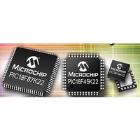
PIC18F46K22-I/MV Microchip Technology, PIC18F46K22-I/MV Datasheet - Page 329

PIC18F46K22-I/MV
Manufacturer Part Number
PIC18F46K22-I/MV
Description
64KB, Flash, 3968bytes-RAM,8-bit Family,nanoWatt XLP 40 UQFN 5x5x0.5mm TUBE
Manufacturer
Microchip Technology
Series
PIC® XLP™ 18Fr
Datasheet
1.PIC18F26J13-ISS.pdf
(496 pages)
Specifications of PIC18F46K22-I/MV
Core Processor
PIC
Core Size
8-Bit
Speed
64MHz
Connectivity
I²C, SPI, UART/USART
Peripherals
Brown-out Detect/Reset, HLVD, POR, PWM, WDT
Number Of I /o
35
Program Memory Size
64KB (32K x 16)
Program Memory Type
FLASH
Eeprom Size
1K x 8
Ram Size
3.8K x 8
Voltage - Supply (vcc/vdd)
1.8 V ~ 5.5 V
Data Converters
A/D 30x10b
Oscillator Type
Internal
Operating Temperature
-40°C ~ 85°C
Package / Case
40-UFQFN Exposed Pad
Processor Series
PIC18F
Core
PIC
Data Bus Width
8 bit
Data Ram Size
4 KB
Number Of Programmable I/os
36
Number Of Timers
3 x 8-bit. 4 x 16-bit
Operating Supply Voltage
1.8 V to 5.5 V
Mounting Style
SMD/SMT
Lead Free Status / RoHS Status
Lead free / RoHS Compliant
Lead Free Status / RoHS Status
Lead free / RoHS Compliant
- Current page: 329 of 496
- Download datasheet (5Mb)
19.9
Upon Reset, all registers of the CTMU are cleared. This
leaves the CTMU module disabled, its current source is
turned off and all configuration options return to their
default settings. The module needs to be re-initialized
following any Reset.
If the CTMU is in the process of taking a measurement at
the time of Reset, the measurement will be lost. A partial
charge may exist on the circuit that was being measured,
and should be properly discharged before the CTMU
makes subsequent attempts to make a measurement.
The circuit is discharged by setting and then clearing the
IDISSEN bit (CTMUCONH<1>) while the A/D Converter
is connected to the appropriate channel.
REGISTER 19-1:
2010 Microchip Technology Inc.
bit 7
Legend:
R = Readable bit
-n = Value at POR
bit 7
bit 6
bit 5
bit 4
bit 3
bit 2
bit 1
bit 0
CTMUEN
R/W-0
Effects of a Reset on CTMU
CTMUEN: CTMU Enable bit
1 = Module is enabled
0 = Module is disabled
Unimplemented: Read as ‘0’
CTMUSIDL: Stop in Idle Mode bit
1 = Discontinue module operation when device enters Idle mode
0 = Continue module operation in Idle mode
TGEN: Time Generation Enable bit
1 = Enables edge delay generation
0 = Disables edge delay generation
EDGEN: Edge Enable bit
1 = Edges are not blocked
0 = Edges are blocked
EDGSEQEN: Edge Sequence Enable bit
1 = Edge 1 event must occur before Edge 2 event can occur
0 = No edge sequence is needed
IDISSEN: Analog Current Source Control bit
1 = Analog current source output is grounded
0 = Analog current source output is not grounded
CTTRIG: CTMU Special Event Trigger Control Bit
1 = CTMU Special Event Trigger is enabled
0 = CTMU Special Event Trigger is disabled
U-0
—
CTMUCONH: CTMU CONTROL REGISTER 0
W = Writable bit
‘1’ = Bit is set
CTMUSIDL
R/W-0
R/W-0
TGEN
Preliminary
U = Unimplemented bit, read as ‘0’
‘0’ = Bit is cleared
EDGEN
R/W-0
19.10 Registers
There are three control registers for the CTMU:
• CTMUCONH
• CTMUCONL
• CTMUICON
The
(Register 19-1
for configuring the CTMU module edge source selec-
tion, edge source polarity selection, edge sequencing,
A/D trigger, analog circuit capacitor discharge and
enables. The CTMUICON register
bits for selecting the current source range and current
source trim.
PIC18(L)F2X/4XK22
CTMUCONH
EDGSEQEN
R/W-0
and
Register
and
x = Bit is unknown
IDISSEN
19-2) contain control bits
R/W-0
CTMUCONL
(Register
DS41412D-page 329
CTTRIG
19-3) has
U-0
registers
bit 0
Related parts for PIC18F46K22-I/MV
Image
Part Number
Description
Manufacturer
Datasheet
Request
R

Part Number:
Description:
Manufacturer:
Microchip Technology Inc.
Datasheet:

Part Number:
Description:
Manufacturer:
Microchip Technology Inc.
Datasheet:

Part Number:
Description:
Manufacturer:
Microchip Technology Inc.
Datasheet:

Part Number:
Description:
Manufacturer:
Microchip Technology Inc.
Datasheet:

Part Number:
Description:
Manufacturer:
Microchip Technology Inc.
Datasheet:

Part Number:
Description:
Manufacturer:
Microchip Technology Inc.
Datasheet:

Part Number:
Description:
Manufacturer:
Microchip Technology Inc.
Datasheet:

Part Number:
Description:
Manufacturer:
Microchip Technology Inc.
Datasheet:


