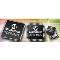
PIC18F46K22-I/MV Microchip Technology, PIC18F46K22-I/MV Datasheet - Page 333

PIC18F46K22-I/MV
Manufacturer Part Number
PIC18F46K22-I/MV
Description
64KB, Flash, 3968bytes-RAM,8-bit Family,nanoWatt XLP 40 UQFN 5x5x0.5mm TUBE
Manufacturer
Microchip Technology
Series
PIC® XLP™ 18Fr
Datasheet
1.PIC18F26J13-ISS.pdf
(496 pages)
Specifications of PIC18F46K22-I/MV
Core Processor
PIC
Core Size
8-Bit
Speed
64MHz
Connectivity
I²C, SPI, UART/USART
Peripherals
Brown-out Detect/Reset, HLVD, POR, PWM, WDT
Number Of I /o
35
Program Memory Size
64KB (32K x 16)
Program Memory Type
FLASH
Eeprom Size
1K x 8
Ram Size
3.8K x 8
Voltage - Supply (vcc/vdd)
1.8 V ~ 5.5 V
Data Converters
A/D 30x10b
Oscillator Type
Internal
Operating Temperature
-40°C ~ 85°C
Package / Case
40-UFQFN Exposed Pad
Processor Series
PIC18F
Core
PIC
Data Bus Width
8 bit
Data Ram Size
4 KB
Number Of Programmable I/os
36
Number Of Timers
3 x 8-bit. 4 x 16-bit
Operating Supply Voltage
1.8 V to 5.5 V
Mounting Style
SMD/SMT
Lead Free Status / RoHS Status
Lead free / RoHS Compliant
Lead Free Status / RoHS Status
Lead free / RoHS Compliant
- Current page: 333 of 496
- Download datasheet (5Mb)
20.0
The module consists of a single SR Latch with multiple
Set and Reset inputs as well as separate latch outputs.
The SR Latch module includes the following features:
• Programmable input selection
• SR Latch output is available internally/externally
• Selectable Q and Q output
• Firmware Set and Reset
The SR Latch can be used in a variety of analog
applications, including oscillator circuits, one-shot
circuit, hysteretic controllers, and analog timing
applications.
20.1
The latch is a Set-Reset Latch that does not depend on
a clock source. Each of the Set and Reset inputs are
active-high. The latch can be set or reset by:
• Software control (SRPS and SRPR bits)
• Comparator C1 output (SYNCC1OUT)
• Comparator C2 output (SYNCC2OUT)
• SRI Pin
• Programmable clock (DIVSRCLK)
The SRPS and the SRPR bits of the SRCON0 register
may be used to set or reset the SR Latch, respectively.
The latch is Reset-dominant. Therefore, if both Set and
Reset inputs are high, the latch will go to the Reset
state. Both the SRPS and SRPR bits are self resetting
which means that a single write to either of the bits is
all that is necessary to complete a latch Set or Reset
operation.
The output from Comparator C1 or C2 can be used as
the Set or Reset inputs of the SR Latch. The output of
either Comparator can be synchronized to the Timer1
clock
Module”
Gate Control”
An external source on the SRI pin can be used as the
Set or Reset inputs of the SR Latch.
An internal clock source, DIVSRCLK, is available and it
can periodically set or reset the SR Latch. The
SRCLK<2:0> bits in the SRCON0 register are used to
select the clock source period. The SRSCKE and
SRRCKE bits of the SRCON1 register enable the clock
source to set or reset the SR Latch, respectively.
2010 Microchip Technology Inc.
source.
SR LATCH
Latch Operation
and
Section 12.0 “Timer1/3/5 Module with
for more information.
See
Section 18.0
“Comparator
Preliminary
20.2
The SRQEN and SRNQEN bits of the SRCON0
register control the Q and Q latch outputs. Both of the
SR Latch outputs may be directly output to I/O pins at
the same time. Control is determined by the state of bits
SRQEN and SRNQEN in the SRCON0 register.
The applicable TRIS bit of the corresponding port must
be cleared to enable the port pin output driver.
20.3
The DIVSRCLK clock signal is generated from the
peripheral clock which is pre-scaled by a value
determined by the SRCLK<2:0> bits. See
and
20.4
Upon any device Reset, the SR Latch is not initialized,
and the SRQ and SRNQ outputs are unknown. The
user’s firmware is responsible to initialize the latch
output before enabling it to the output pins.
PIC18(L)F2X/4XK22
Table 20-1
Latch Output
DIVSRCLK Clock Generation
Effects of a Reset
for additional detail.
DS41412D-page 333
Figure 20-2
Related parts for PIC18F46K22-I/MV
Image
Part Number
Description
Manufacturer
Datasheet
Request
R

Part Number:
Description:
Manufacturer:
Microchip Technology Inc.
Datasheet:

Part Number:
Description:
Manufacturer:
Microchip Technology Inc.
Datasheet:

Part Number:
Description:
Manufacturer:
Microchip Technology Inc.
Datasheet:

Part Number:
Description:
Manufacturer:
Microchip Technology Inc.
Datasheet:

Part Number:
Description:
Manufacturer:
Microchip Technology Inc.
Datasheet:

Part Number:
Description:
Manufacturer:
Microchip Technology Inc.
Datasheet:

Part Number:
Description:
Manufacturer:
Microchip Technology Inc.
Datasheet:

Part Number:
Description:
Manufacturer:
Microchip Technology Inc.
Datasheet:


