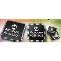
PIC18F46K22-I/MV Microchip Technology, PIC18F46K22-I/MV Datasheet - Page 335

PIC18F46K22-I/MV
Manufacturer Part Number
PIC18F46K22-I/MV
Description
64KB, Flash, 3968bytes-RAM,8-bit Family,nanoWatt XLP 40 UQFN 5x5x0.5mm TUBE
Manufacturer
Microchip Technology
Series
PIC® XLP™ 18Fr
Datasheet
1.PIC18F26J13-ISS.pdf
(496 pages)
Specifications of PIC18F46K22-I/MV
Core Processor
PIC
Core Size
8-Bit
Speed
64MHz
Connectivity
I²C, SPI, UART/USART
Peripherals
Brown-out Detect/Reset, HLVD, POR, PWM, WDT
Number Of I /o
35
Program Memory Size
64KB (32K x 16)
Program Memory Type
FLASH
Eeprom Size
1K x 8
Ram Size
3.8K x 8
Voltage - Supply (vcc/vdd)
1.8 V ~ 5.5 V
Data Converters
A/D 30x10b
Oscillator Type
Internal
Operating Temperature
-40°C ~ 85°C
Package / Case
40-UFQFN Exposed Pad
Processor Series
PIC18F
Core
PIC
Data Bus Width
8 bit
Data Ram Size
4 KB
Number Of Programmable I/os
36
Number Of Timers
3 x 8-bit. 4 x 16-bit
Operating Supply Voltage
1.8 V to 5.5 V
Mounting Style
SMD/SMT
Lead Free Status / RoHS Status
Lead free / RoHS Compliant
Lead Free Status / RoHS Status
Lead free / RoHS Compliant
- Current page: 335 of 496
- Download datasheet (5Mb)
TABLE 20-1:
REGISTER 20-1:
2010 Microchip Technology Inc.
bit 7
Legend:
R = Readable bit
-n = Value at POR
bit 7
bit 6-4
bit 3
bit 2
bit 1
bit 0
Note 1:
SRCLK<2:0>
SRLEN
R/W-0
111
110
101
100
011
010
001
000
2:
Changing the SRCLK bits while the SR latch is enabled may cause false triggers to the set and Reset
inputs of the latch.
Set only, always reads back ‘0’.
SRLEN: SR Latch Enable bit
1 = SR latch is enabled
0 = SR latch is disabled
SRCLK<2:0>: SR Latch Clock Divider Bits
000 = Generates a 2 T
001 = Generates a 2 T
010 = Generates a 2 T
011 = Generates a 2 T
100 = Generates a 2 T
101 = Generates a 2 T
110 = Generates a 2 T
111 = Generates a 2 T
SRQEN: SR Latch Q Output Enable bit
1 = Q is present on the SRQ pin
0 = Q is internal only
SRNQEN: SR Latch Q Output Enable bit
1 = Q is present on the SRNQ pin
0 = Q is internal only
SRPS: Pulse Set Input of the SR Latch bit
1 = Pulse set input for 2 T
0 = No effect on set input
SRPR: Pulse Reset Input of the SR Latch bit
1 = Pulse reset input for 2 T
0 = No effect on Reset input
DIVSRCLK FREQUENCY TABLE
Divider
R/W-0
512
256
128
64
32
16
8
4
SRCON0: SR LATCH CONTROL REGISTER
SRCLK<2:0>
F
W = Writable bit
‘1’ = Bit is set
OSC
R/W-0
25.6 s
12.8 s
6.4 s
3.2 s
1.6 s
0.8 s
0.4 s
0.2 s
= 20 MHz
OSC
OSC
OSC
OSC
OSC
OSC
OSC
OSC
OSC
OSC
wide pulse on DIVSRCLK every 4 peripheral clock cycles
wide pulse on DIVSRCLK every 16 peripheral clock cycles
wide pulse on DIVSRCLK every 32 peripheral clock cycles
wide pulse on DIVSRCLK every 64 peripheral clock cycles
wide pulse on DIVSRCLK every 128 peripheral clock cycles
wide pulse on DIVSRCLK every 256 peripheral clock cycles
wide pulse on DIVSRCLK every 512 peripheral clock cycles
(1)
wide pulse on DIVSRCLK every 8 peripheral clock cycles
clock cycles
R/W-0
clock cycles
F
Preliminary
OSC
0.25 s
0.5 s
32 s
16 s
8 s
4 s
2 s
1 s
= 16 MHz
(2)
U = Unimplemented
‘0’ = Bit is cleared
(2)
SRQEN
R/W-0
PIC18(L)F2X/4XK22
F
OSC
0.5 s
64 s
32 s
16 s
8 s
4 s
2 s
1 s
= 8 MHz F
SRNQEN
R/W-0
OSC
128 s
C = Clearable only bit
x = Bit is unknown
64 s
32 s
16 s
8 s
4 s
2 s
1 s
= 4 MHz
R/W-0
SRPS
DS41412D-page 335
F
OSC
512 s
256 s
128 s
64 s
32 s
16 s
R/W-0
SRPR
8 s
4 s
= 1 MHz
bit 0
Related parts for PIC18F46K22-I/MV
Image
Part Number
Description
Manufacturer
Datasheet
Request
R

Part Number:
Description:
Manufacturer:
Microchip Technology Inc.
Datasheet:

Part Number:
Description:
Manufacturer:
Microchip Technology Inc.
Datasheet:

Part Number:
Description:
Manufacturer:
Microchip Technology Inc.
Datasheet:

Part Number:
Description:
Manufacturer:
Microchip Technology Inc.
Datasheet:

Part Number:
Description:
Manufacturer:
Microchip Technology Inc.
Datasheet:

Part Number:
Description:
Manufacturer:
Microchip Technology Inc.
Datasheet:

Part Number:
Description:
Manufacturer:
Microchip Technology Inc.
Datasheet:

Part Number:
Description:
Manufacturer:
Microchip Technology Inc.
Datasheet:


