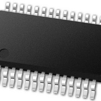
PIC24FJ64GB002-I/SS Microchip Technology, PIC24FJ64GB002-I/SS Datasheet - Page 320

PIC24FJ64GB002-I/SS
Manufacturer Part Number
PIC24FJ64GB002-I/SS
Description
16-bit, 16 MIPS, 64KB Flash, 8KB RAM, Nanowatt XLP, USB OTG 28 SSOP .209in TUBE
Manufacturer
Microchip Technology
Specifications of PIC24FJ64GB002-I/SS
Processor Series
PIC24
Core
PIC24F
Data Bus Width
16 bit
Program Memory Type
Flash
Program Memory Size
64 KB
Data Ram Size
8192 B
Interface Type
I2C, SPI, UART
Maximum Clock Frequency
32 MHz
Number Of Programmable I/os
21
Number Of Timers
5
Operating Supply Voltage
2 V to 3.6 V
Maximum Operating Temperature
+ 85 C
Mounting Style
SMD/SMT
Package / Case
SSOP-28
Development Tools By Supplier
MPLAB Integrated Development Environment
Minimum Operating Temperature
- 40 C
Operating Temperature Range
- 40 C to + 85 C
Supply Current (max)
300 mA
Lead Free Status / Rohs Status
Lead free / RoHS Compliant
Available stocks
Company
Part Number
Manufacturer
Quantity
Price
Part Number:
PIC24FJ64GB002-I/SS
Manufacturer:
MICROCHIP/微芯
Quantity:
20 000
- Current page: 320 of 352
- Download datasheet (3Mb)
PIC24FJ64GB004 FAMILY
FIGURE 29-4:
TABLE 29-16: EXTERNAL CLOCK TIMING REQUIREMENTS
DS39940D-page 320
AC CHARACTERISTICS
OS10
OS20
OS25
OS30
OS31
OS40
OS41
Note 1:
Param
No.
CLKO
OSCI
2:
3:
F
T
T
TosL,
TosH
TosR,
TosF
TckR CLKO Rise Time
TckF
Sym
OSC
CY
OSC
Data in “Typ” column is at 3.3V, 25°C unless otherwise stated. Parameters are for design guidance only
and are not tested.
Instruction cycle period (T
are based on characterization data for that particular oscillator type under standard operating conditions
with the device executing code. Exceeding these specified limits may result in an unstable oscillator
operation and/or higher than expected current consumption. All devices are tested to operate at “Min.”
values with an external clock applied to the OSCI/CLKI pin. When an external clock input is used, the
“Max.” cycle time limit is “DC” (no clock) for all devices.
Measurements are taken in EC mode. The CLKO signal is measured on the OSCO pin. CLKO is low for
the Q1-Q2 period (1/2 T
External CLKI Frequency
(External clocks allowed
only in EC mode)
Oscillator Frequency
T
Instruction Cycle Time
External Clock in (OSCI)
High or Low Time
External Clock in (OSCI)
Rise or Fall Time
CLKO Fall Time
OSC
Q4
= 1/F
Characteristic
EXTERNAL CLOCK TIMING
OSC
Q1
(3)
(3)
Q2
CY
OS25
CY
) and high for the Q3-Q4 period (1/2 T
(2)
OS20
) equals two times the input oscillator time base period. All specified values
Q3
OS40
Standard Operating Conditions: 2.50 to 3.6V (unless otherwise stated)
Operating temperature
0.45 x T
62.5
Min
DC
DC
10
31
10
—
—
—
—
4
4
3
3
3
Q4
OSC
Q1
Typ
—
—
—
—
—
—
—
—
—
—
—
—
—
—
6
6
(1)
OS30
Q2
Max
DC
-40°C T
-40°C T
32
24
10
32
33
24
20
10
10
—
—
8
6
8
6
OS30
Q3
CY
OS41
).
Units
MHz
MHz
MHz
MHz
MHz
MHz
MHz
MHz
MHz
kHz
A
A
ns
ns
ns
ns
ns
—
Q4
+85°C for Industrial
+125°C for Extended
EC, -40°C T
ECPLL, -40°C T
EC, -40°C T
ECPLL, -40°C T
XT
XTPLL, -40°C T
HS, -40°C T
SOSC
XTPLL, -40°C T
HS, -40°C T
See parameter OS10
for F
EC
EC
2010 Microchip Technology Inc.
Q1
OS31
OSC
Q2
Conditions
value
OS31
A
A
A
A
+85°C
+125°C
+85°C
+125°C
Q3
A
A
A
A
+85°C
+125°C
+85°C
+125°C
Related parts for PIC24FJ64GB002-I/SS
Image
Part Number
Description
Manufacturer
Datasheet
Request
R

Part Number:
Description:
Manufacturer:
Microchip Technology Inc.
Datasheet:

Part Number:
Description:
Manufacturer:
Microchip Technology Inc.
Datasheet:

Part Number:
Description:
Manufacturer:
Microchip Technology Inc.
Datasheet:

Part Number:
Description:
Manufacturer:
Microchip Technology Inc.
Datasheet:

Part Number:
Description:
Manufacturer:
Microchip Technology Inc.
Datasheet:

Part Number:
Description:
Manufacturer:
Microchip Technology Inc.
Datasheet:

Part Number:
Description:
Manufacturer:
Microchip Technology Inc.
Datasheet:

Part Number:
Description:
Manufacturer:
Microchip Technology Inc.
Datasheet:


