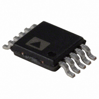
SSM2167-1RMZ-R7 Analog Devices Inc, SSM2167-1RMZ-R7 Datasheet

SSM2167-1RMZ-R7
Specifications of SSM2167-1RMZ-R7
Available stocks
Related parts for SSM2167-1RMZ-R7
SSM2167-1RMZ-R7 Summary of contents
Page 1
... The flexibility of setting the compression ratio and the time constant of the level detector, coupled with two values of rotation point, make the SSM2167 easy to integrate in a wide variety of microphone conditioning applications. The device is available in a 10-lead MSOP package, and is guaranteed for operation over the extended industrial temperature range of − ...
Page 2
... PCB Layout Considerations ...................................................... 10 Outline Dimensions ....................................................................... 11 Ordering Guide .......................................................................... 11 9/03—Rev Rev. B Deleted SSM2167-2 Model ................................................ Universal Changes to Ordering Guide ............................................................. 3 Edits to Figure 2 and Figure 3 .......................................................... 6 Updated Outline Dimensions .......................................................... 9 3/02—Rev Rev. A Edits to Specifications ....................................................................... 2 Edits to Figure 2 and Figure 3 .......................................................... 6 7/01—Revision 0: Initial Version Rev Page ...
Page 3
... PSRR Pin 3 = GND SY Rev Page kΩ, unless otherwise noted. GATE Min Typ Max 20 −70 0.2 100 145 5 2 600 700 1:1 10:1 63 −40 2.5 5.5 2 SSM2167 Unit nV/√Hz dBV % kΩ Ω kΩ rms mV rms MHz rms dBV μA ...
Page 4
... SSM2167 ABSOLUTE MAXIMUM RATINGS Table 2. Parameter Supply Voltage Input Voltage Operating Temperature Range Storage Temperature Range Junction Temperature Lead Temperature (Soldering, 10 sec) 883 (Human Body) Model Stresses above those listed under Absolute Maximum Ratings may cause permanent damage to the device. This is a stress rating only ...
Page 5
... 100kΩ LOAD ROTATION POINT = 63mV rms NOISE GATE SETTING = 2mV rms –80 –70 –60 –50 –40 –30 INPUT (dBV) Figure 7. Output vs. Input Characteristics 0 5kΩ GATE R = 0Ω COMP 10 100 1k 10k FREQUENCY (Hz) Figure 8. PSRR vs. Frequency SSM2167 1 –20 –10 100k ...
Page 6
... SSM2167 T = 25° 10µF SYS SYSTEM GAIN = 19dB R = 100kΩ LOAD COMPRESSION RATIO 1:1 TIME (10µs/DIV) Figure 9. Small Signal Transient Response T = 25° 10µF SYS SYSTEM GAIN = 8.6dB R = 100kΩ LOAD COMPRESSION RATIO 1:1 TIME (10µs/DIV) Figure 10. Large Signal Transient Response T = 25° ...
Page 7
... TIME (1s/DIV) Figure 13. RMS Level Detector Performance with C –6dBV –66dBV –85dBV = 22 μF Figure 14. RMS Level Detector Performance with C AVG Rev Page SSM2167 –6dBV –66dBV –85dBV TIME (500ms/DIV) = 2.2 μF AVG ...
Page 8
... the SSM2167. The net gain from input to output can be as high as 40 dB, depending on the gain set by the control circuitry. The output impedance of the SSM2167 is typically less than 145 Ω, and the external load on Pin 9 should be >5 kΩ. The nominal output dc voltage of the device is approximately 1.4 V ...
Page 9
... Figure 14 for 2.2 μF and Figure 13 for a C AVG In Figure 13 and Figure 14, the input signal to the SSM2167 (not shown series of tone bursts in six successive 10 dB steps. The tone bursts range from −66 dBV (0.5 mV rms) to −6 dBV (0.5 V rms). As illustrated in these figures, the attack ...
Page 10
... VCA GAIN should be considered for the PCB. The layout should minimize possible capacitive feedback from the output of the SSM2167 back to its input. Do not run input and output traces adjacent to each other. A single-point (star) ground implementation is recommended in addition to maintaining short lead lengths and PCB runs. In ...
Page 11
... OUTLINE DIMENSIONS IDENTIFIER ORDERING GUIDE 1 Model Temperature Range SSM2167-1RMZ-REEL −40°C to +85°C SSM2167-1RMZ-R7 −40°C to +85°C SSM2167Z-EVAL RoHS Compliant Part, # denotes RoHS compliant product may be top or bottom marked. 3.10 3.00 2.90 5. 3.10 4.90 3.00 4.65 1 2.90 5 PIN 1 0.50 BSC 0.95 15° ...
Page 12
... SSM2167 NOTES ©2001–2011 Analog Devices, Inc. All rights reserved. Trademarks and registered trademarks are the property of their respective owners. D02628-0-2/11(F) Rev Page ...


