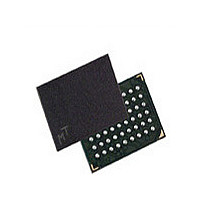
MT45W8MW16BGX-701 IT Micron Technology Inc, MT45W8MW16BGX-701 IT Datasheet - Page 36

MT45W8MW16BGX-701 IT
Manufacturer Part Number
MT45W8MW16BGX-701 IT
Description
Manufacturer
Micron Technology Inc
Datasheet
1.MT45W8MW16BGX-701_IT.pdf
(68 pages)
Specifications of MT45W8MW16BGX-701 IT
Operating Temperature (max)
85C
Operating Temperature (min)
-40C
Mounting
Surface Mount
Operating Temperature Classification
Industrial
Lead Free Status / RoHS Status
Compliant
- Current page: 36 of 68
- Download datasheet (2Mb)
Table 12:
Table 13:
Figure 26:
Figure 27:
PDF: 09005aef80ec6f79/Source: 09005aef80ec6f65
128mb_burst_cr1_5_p26z__2.fm - Rev. H 9/07 EN
Description
Description
Deep Power-Down
Input Capacitance
Input/Output Capacitance
(DQ)
Deep Power-Down Specifications
Typical (TYP) I
Capacitance
These parameters are verified in device characterization and are not 100-percent tested
AC Input/Output Reference Waveform
AC Output Load Circuit
Notes:
Notes:
ZZ
Input
1. AC test inputs are driven at V
2. Input timing begins at V
3. Output timing ends at V
1. All tests are performed with the outputs configured for default setting of half drive
value applies across all operating temperatures and voltages
DUT
V
times (10 percent to 90 percent) <1.6ns.
strength (BCR[5:4] = 01b).
V
CC
SS
1
Q
Q
V
CC
T
C
, V
128Mb: 8 Meg x 16 Async/Page/Burst CellularRAM 1.5 Async/
V
= +25ºC; f = 1 MHz;
IN
V
CC
Conditions
Conditions
CC
Test Point
= V
Q = 1.95V; +85°C
V
Q/2
IN
CC
= 0V
2
Q or 0V;
30pF
50Ω
CC
CC
Q/2.
Q/2.
36
CC
VccQ/2
Q for a logic 1 and V
Test Points
Symbol
Symbol
C
C
I
ZZ
IO
IN
Micron Technology, Inc., reserves the right to change products or specifications without notice.
Page/Burst CellularRAM 1.5 Memory
Min
Typ
SS
2.0
3.5
3
Q for a logic 0. Input rise and fall
V
CC
Q/2
©2004 Micron Technology, Inc. All rights reserved.
3
Max
Max
Output
10
6
6
Units
Unit
µA
pF
pF
Related parts for MT45W8MW16BGX-701 IT
Image
Part Number
Description
Manufacturer
Datasheet
Request
R

Part Number:
Description:
IC SDRAM 64MBIT 133MHZ 54TSOP
Manufacturer:
Micron Technology Inc
Datasheet:

Part Number:
Description:
IC SDRAM 64MBIT 5.5NS 86TSOP
Manufacturer:
Micron Technology Inc
Datasheet:

Part Number:
Description:
IC SDRAM 64MBIT 200MHZ 86TSOP
Manufacturer:
Micron Technology Inc
Datasheet:

Part Number:
Description:
IC SDRAM 64MBIT 133MHZ 54TSOP
Manufacturer:
Micron Technology Inc
Datasheet:

Part Number:
Description:
IC SDRAM 128MBIT 133MHZ 54TSOP
Manufacturer:
Micron Technology Inc
Datasheet:

Part Number:
Description:
IC SDRAM 256MBIT 133MHZ 90VFBGA
Manufacturer:
Micron Technology Inc
Datasheet:

Part Number:
Description:
IC SDRAM 128MBIT 133MHZ 54TSOP
Manufacturer:
Micron Technology Inc
Datasheet:

Part Number:
Description:
IC SDRAM 256MBIT 133MHZ 54TSOP
Manufacturer:
Micron Technology Inc
Datasheet:

Part Number:
Description:
IC DDR SDRAM 512MBIT 6NS 66TSOP
Manufacturer:
Micron Technology Inc
Datasheet:

Part Number:
Description:
IC SDRAM 128MBIT 167MHZ 86TSOP
Manufacturer:
Micron Technology Inc
Datasheet:

Part Number:
Description:
IC SDRAM 128MBIT 143MHZ 86TSOP
Manufacturer:
Micron Technology Inc
Datasheet:

Part Number:
Description:
SDRAM 256M-BIT 1.8V 54-PIN VFBGA
Manufacturer:
Micron Technology Inc
Datasheet:

Part Number:
Description:
IC SDRAM 128MBIT 143MHZ 86TSOP
Manufacturer:
Micron Technology Inc
Datasheet:

Part Number:
Description:
IC SDRAM 128MBIT 125MHZ 54VFBGA
Manufacturer:
Micron Technology Inc
Datasheet:

Part Number:
Description:
IC SDRAM 128MBIT 125MHZ 54VFBGA
Manufacturer:
Micron Technology Inc
Datasheet:


