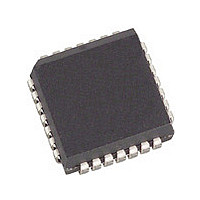
CY7C291A-35JCT Cypress Semiconductor Corp, CY7C291A-35JCT Datasheet

CY7C291A-35JCT
Specifications of CY7C291A-35JCT
Available stocks
Related parts for CY7C291A-35JCT
CY7C291A-35JCT Summary of contents
Page 1
... The memory cells utilize proven EPROM floating-gate technology programming algorithms. The CY7C291A is a plug-in replacement for bipolar devices and offers the advantage of lower power, reprogrammability, superior performance and programming yield. The EPROM cell requires only 12.5V for the supervoltage and low current requirements allow for gang programming ...
Page 2
... DC Program Voltage..................................................... 13.0V UV Exposure ................................................ 7258 Wsec/cm Static Discharge Voltage............................................ >2001V (per MIL-STD-883, Method 3015) Latch-Up Current ..................................................... >200 mA Operating Range Range Temperature ° Commercial 0 ° −55 [1] Military CY7C291A 7C291A-50 Unit Ambient V CC ° 5V ±10 ° 5V ±10 125 C Page [+] Feedbac ...
Page 3
... −10 GND < V < OUT CC Output Disabled − Max GND CC OUT V = Max., Com’ OUT V = Max., Com’ 3.0 CY7C291A 7C291A-25 Max. Min. Max. Unit 2.4 V 0 0.8 0.8 V −10 µA +10 +10 Note 3 −10 µA +10 +10 −90 −20 −90 mA 120 ...
Page 4
... GND CC OUT V = Max., Commercial 2.0V IN Military OUT V = Max., Commercial Military Test Conditions T = 25° MHz 5.0V CC CY7C291A 7C291A-35 7C291AL-35 7C291A-50 Min. Max. Min. Max. Unit 2.4 2.4 V 0.4 0.4 V 2.0 2.0 V 0.8 0.8 V −10 −10 µA +10 +10 Note 3 −10 −10 µA ...
Page 5
... Chip Select Inactive to Power-Down PD Document #: 38-04011 Rev. *B [3] R1250 Ω GND 167Ω JIG AND SCOPE (b) High Z Load 2. 50% t HZCS [2, 3] 7C291A-20 7C291A-25 Min. Max. Min. Max CY7C291A ALL INPUT PULSES 90% 90% 10% 10% < < 50% t ACS 7C291A-35 7C291A-50 7C291AL-35 Min. Max. Min. Max ...
Page 6
... IHP − ILP − IHP Figure 1. Programming Pinouts LCC/PLCC (Opaque Only) Top View 7C291A VFY PGM 1314151617 CY7C291A 2 is the recommended maximum dosage. [5] − −D VFY − High High High Z − IHP − ILP High Z IHP PP − IHP Zeros ILP ...
Page 7
... OUTPUT VOLTAGE (V) I vs. CYCLE PERIOD CC 1.02 1.00 0.98 0.96 0.94 0.92 0.90 0.88 3.0 4 CYCLE PERIOD (ns) CY7C291A NORMALIZED ACCESS TIME vs. SUPPLY VOLTAGE 1.2 1.0 0.8 0.6 T =25°C A 0.4 4.0 4.5 5.0 5.5 SUPPLY VOLTAGE (V) TYPICAL ACCESS TIME CHANGE vs. OUTPUT LOADING 30 ...
Page 8
... Molded DIP W14 24-Lead (300-Mil) Windowed CerDIP SMD Cross Reference Subgroups SMD Number 5962-87650 5962-87650 5962-88734 5962-88734 5962-88734 5962-88734 Subgroups CY7C291A Operating Range Commercial Commercial Commercial Commercial Military Commercial Military Cypress Suffix Number 01LX CY7C291-50WMB 03LX CY7C291-35WMB 023X CY7C291A-35LMB 033X CY7C291A-35LMB 04LX ...
Page 9
... Package Diagrams Figure 2. 24-Lead (300-Mil) CerDIP D14 Figure 3. 24-Lead (300-Mil) PDIP P13 Document #: 38-04011 Rev. *B MIL-STD-1835 D- 9 Config.A CY7C291A 51-80031-** 51-85013-*B Page [+] Feedbac ...
Page 10
... Package Diagrams (continued) Figure 4. 28-Pin Windowed Leadless Chip Carrier Q64 Document #: 38-04011 Rev. *B MIL–STD–1835 C–4 51-80102-** CY7C291A Page [+] Feedbac ...
Page 11
... DOES INCLUDE MOLD MISMATCH AND ARE MEASURED AT THE MOLD PARTING LINE. MOLD PROTRUSION/END FLASH SHALL NOT EXCEED 0.010 in (0.254 mm) PER SIDE 3. DIMENSIONS IN INCHES 4. PACKAGE WEIGHT 0.65gms * 0.394[10.007] 0.419[10.642] SEATING PLANE 0.092[2.336] 0.105[2.667] 0.004[0.101] * CY7C291A MIN. MAX. PART # S24.3 STANDARD PKG. SZ24.3 LEAD FREE PKG. 0.0091[0.231] 0.015[0.381] 0.0125[0.317] 0.050[1.270] 51-85025-*C Page ...
Page 12
... The inclusion of Cypress products in life-support systems application implies that the manufacturer assumes all risk of such use and in doing so indemnifies Cypress against all charges. MIL-STD-1835 D-9 Config. A CY7C291A 51-80086-** Page ...
Page 13
... Document History Page Document Title: CY7C291A Reprogrammable PROM Document Number: 38-04011 Issue REV. ECN NO. Date ** 114138 03/18/02 *A 118905 10/11/02 *B 499562 See ECN Document #: 38-04011 Rev. *B Orig. of Change DSG Changed from Spec number: 38-00075 to 38-04011 GBI Updated ordering information PCI Updated ordering information ...


