HV5408PJ-B-G Supertex, HV5408PJ-B-G Datasheet
HV5408PJ-B-G
Specifications of HV5408PJ-B-G


Related parts for HV5408PJ-B-G


HV5408PJ-B-G Summary of contents
Page 1
... Transfer of data from the shift register to the latch occurs when the LE input is high. The data in the latch is retained when LE is low High Voltage Level Translators & Latches Push-Pull Output Buffers Supertex HV5408B ● 1235 Bordeaux Drive, Sunnyvale, CA 94089 HV5408B HV 1 OUT Columns HV 32 Display OUT Panel ● Tel: 408-222-8888 ● ...
Page 2
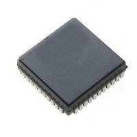
... CCCCCCCC AAA *May be part of top marking 44-Lead PQFP (PG) Packages may or may not include the following marks ● 1235 Bordeaux Drive, Sunnyvale, CA 94089 2 44-Lead PLCC .653x.653in body .180in height (max) .050in pitch HV5408PJ-B 44-Lead Quad Cerpac (DJ) (top view 44-Lead PQFP (PG) (top view ...
Page 3
... Current leakage, any input output clamp diode voltage output when sourcing output when sinking output when sourcing output when sinking OL Supertex inc. (over -40°C to 85°C for plastic and -55°C to 125°C for ceramic) 10 float during operation 60V 12V 25° Min Max Units - 0 ...
Page 4
... Width of LE pulse WLE t LE setup time before CLK SLE t Delay from OUT t Delay from OFF OUT Switching Waveforms 50% DATA INPUT 50% CLK DATA OUT LE HV OUT w/ S/R LOW HV OUT w/ S/R HIGH Supertex inc. Min Max Units - 8.0 MHz 110 - 110 500 ...
Page 5
... INPUT CLK Register DATA OUT Function Tables DATA INPUT CLK Note LOW - to - HIGH transition H = High L = Low X = Don’t Care Supertex inc. VDD GND Logic Data Output 32 bit 32 bit Static Latches DATA OUT DATA INPUT change H L ● 1235 Bordeaux Drive, Sunnyvale, CA 94089 ...
Page 6
... CLK 28 GND 29 VPP 30 VDD Supertex inc. Description High voltage outputs. High voltage push-pull outputs, which, depending on controlling low voltage data, can drive loads either to GND Serial data output. Data output for cascading to the data input of the next device. No connect. Data shift register clock Input are shifted into the shift register on the positive edge of the clock ...
Page 7
... OUT OUT Supertex inc. Description Latch enable input. When LE is HIGH, shift register data is transferred into a data latch. When LE is LOW, data is latched, and new data can be clocked into the shift register. Serial data input. Data needs to be present before each rising edge of the clock. ...
Page 8
... VPP 25 VDD DATA INPUT Supertex inc. Description High voltage outputs. High voltage push-pull outputs, which, depending on controlling low voltage data, can drive loads either to GND Serial data output. Data output for cascading to the data input of the next device. No connect. Data shift register clock Input are shifted into the shift register on the positive edge of the clock ...
Page 9
... HV 14 OUT OUT Supertex inc. Description Output enable input. When OE is LOW, all HV outputs are forced into a LOW state, regardless of data in each channel. When OE is HIGH, all HV outputs reflect data latched. No connect. High voltage outputs. High voltage push-pull outputs, which, depending on controlling low voltage data, can drive loads either to GND ● ...
Page 10
... A Pin 1 identifier must be located in the index area indicated. The Pin 1 identifier can be: a molded mark/identifier; an embedded metal marker printed indicator. Symbol A MIN .155 Dimension NOM .172 (inches) MAX .190 JEDEC Registration MO-087, Variation AB, Issue B, August, 1991. Drawings not to scale. Supertex Doc. #: DSPD-44CERPACDJ, Version D090808. Supertex inc Note 1 (Index Area) E1 Top View View B Seating Plane ...
Page 11
... A A1 MIN 1.95* 0.00 Dimension NOM - - (mm) MAX 2.35 0.25 JEDEC Registration MO-112, Variation AA-2, Issue B, Sep.1995. * This dimension is not specified in the JEDEC drawing. Drawings not to scale. Supertex Doc. #: DSPD-44PQFPPG, Version C041309. Supertex inc View B Seating Plane 1.95 0.30 13.65* 9.80* 2 ...
Page 12
... JEDEC Registration MS-018, Variation AC, Issue A, June, 1993. † This dimension differs from the JEDEC drawing. Drawings not to scale. Supertex Doc. #: DSPD-44PLCCPJ, Version E041309. (The package drawing(s) in this data sheet may not reflect the most current specifications. For the latest package outline information go to supertex.com/packaging.html.) does not recommend the use of its products in life support applications, and will not knowingly sell them for use in such applications unless it receives Supertex inc ...