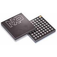
LPC1778FET208,551 NXP Semiconductors, LPC1778FET208,551 Datasheet - Page 13

LPC1778FET208,551
Manufacturer Part Number
LPC1778FET208,551
Description
MCU ARM 512K FLASH 208-TFBGA
Manufacturer
NXP Semiconductors
Series
LPC17xxr
Specifications of LPC1778FET208,551
Core Processor
ARM® Cortex-M3™
Core Size
32-Bit
Speed
100MHz
Connectivity
CAN, EBI/EMI, Ethernet, I²C, Microwire, MMC, SPI, SSI, SSP, UART/USART, USB OTG
Peripherals
Brown-out Detect/Reset, DMA, I²S, Motor Control PWM, POR, PWM, WDT
Number Of I /o
165
Program Memory Size
512KB (512K x 8)
Program Memory Type
FLASH
Eeprom Size
4K x 8
Ram Size
96K x 8
Voltage - Supply (vcc/vdd)
2.4 V ~ 3.6 V
Data Converters
A/D 8x12b, D/A 1x10b
Oscillator Type
Internal
Operating Temperature
-40°C ~ 85°C
Package / Case
208-TFBGA
Processor Series
LPC177x
Core
ARM Cortex M3
Data Bus Width
32 bit
Data Ram Size
96 KB
Interface Type
SSP, I2S, USB, JTAG, Serial, UART, I2C, SD/MMC
Maximum Clock Frequency
100 MHz
Number Of Programmable I/os
165
Number Of Timers
4
Operating Supply Voltage
2.4 V to 3.6 V
Maximum Operating Temperature
+ 85 C
Mounting Style
SMD/SMT
Operating Temperature Range
- 40 C to + 85 C
Supply Current (max)
100 mA
Lead Free Status / Rohs Status
Lead free / RoHS Compliant
Other names
568-6688
Available stocks
Company
Part Number
Manufacturer
Quantity
Price
Company:
Part Number:
LPC1778FET208,551
Manufacturer:
NXP Semiconductors
Quantity:
10 000
NXP Semiconductors
Table 3.
Not all functions are available on all parts. See
pins).
LPC178X_7X
Objective data sheet
Symbol
P0[11]
P0[12]
P0[13]
P0[14]
P0[15]
P0[16]
P0[17]
Pin description
100 R14
41
45
69
128 J16
130 J14
126 K17
R1
R2
T7
…continued
P12
J4
J5
M5
H13 89
H14 90
J12
70
29
32
48
87
[3]
[5]
[5]
[3]
[3]
[3]
[3]
All information provided in this document is subject to legal disclaimers.
I;
PU
I;
PU
I;
PU
I;
PU
I;
PU
I;
PU
I;
PU
Table 2
Rev. 2 — 27 May 2011
I/O
I
I/O
O
-
-
-
O
I/O
O
I/O
I
I/O
O
I/O
I
I/O
O
I/O
O
I/O
O
I/O
I/O
I
I/O
I/O
I
I/O
(Ethernet, USB, LCD, QEI, SD/MMC, DAC pins) and
Description
P0[11] — General purpose digital input/output pin.
U2_RXD — Receiver input for UART2.
I2C2_SCL — I
specialized I2C pad).
T3_MAT1 — Match output for Timer 3, channel 1.
R — Function reserved.
R — Function reserved.
R — Function reserved.
LCD_VD[10] — LCD data.
P0[12] — General purpose digital input/output pin.
USB_PPWR2 — Port Power enable signal for USB port 2.
SSP1_MISO — Master In Slave Out for SSP1.
ADC0_IN[6] — A/D converter 0, input 6. When configured as an
ADC input, the digital function of the pin must be disabled.
P0[13] — General purpose digital input/output pin.
USB_UP_LED2 — USB port 2 GoodLink LED indicator. It is
LOW when device is configured (non-control endpoints
enabled). It is HIGH when the device is not configured or during
global suspend.
SSP1_MOSI — Master Out Slave In for SSP1.
ADC0_IN[7] — A/D converter 0, input 7. When configured as an
ADC input, the digital function of the pin must be disabled.
P0[14] — General purpose digital input/output pin.
USB_HSTEN2 — Host Enabled status for USB port 2.
SSP1_SSEL — Slave Select for SSP1.
USB_CONNECT2 — SoftConnect control for USB port 2.
Signal used to switch an external 1.5 k resistor under software
control. Used with the SoftConnect USB feature.
P0[15] — General purpose digital input/output pin.
U1_TXD — Transmitter output for UART1.
SSP0_SCK — Serial clock for SSP0.
P0 [16] — General purpose digital input/output pin.
U1_RXD — Receiver input for UART1.
SSP0_SSEL — Slave Select for SSP0.
P0[17] — General purpose digital input/output pin.
U1_CTS — Clear to Send input for UART1.
SSP0_MISO — Master In Slave Out for SSP0.
2
C2 clock input/output (this pin does not use a
32-bit ARM Cortex-M3 microcontroller
LPC178x/7x
© NXP B.V. 2011. All rights reserved.
Table 7
13 of 117
(EMC


