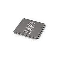
LPC1778FBD208,551 NXP Semiconductors, LPC1778FBD208,551 Datasheet - Page 25

LPC1778FBD208,551
Manufacturer Part Number
LPC1778FBD208,551
Description
MCU ARM 512K FLASH 208-LQFP
Manufacturer
NXP Semiconductors
Series
LPC17xxr
Specifications of LPC1778FBD208,551
Core Processor
ARM® Cortex-M3™
Core Size
32-Bit
Speed
100MHz
Connectivity
CAN, EBI/EMI, Ethernet, I²C, Microwire, MMC, SPI, SSI, SSP, UART/USART, USB OTG
Peripherals
Brown-out Detect/Reset, DMA, I²S, Motor Control PWM, POR, PWM, WDT
Number Of I /o
165
Program Memory Size
512KB (512K x 8)
Program Memory Type
FLASH
Eeprom Size
4K x 8
Ram Size
96K x 8
Voltage - Supply (vcc/vdd)
2.4 V ~ 3.6 V
Data Converters
A/D 8x12b, D/A 1x10b
Oscillator Type
Internal
Operating Temperature
-40°C ~ 85°C
Package / Case
208-LQFP
Processor Series
LPC177x
Core
ARM Cortex M3
Data Bus Width
32 bit
Data Ram Size
96 KB
Interface Type
SSP, I2S, USB, JTAG, Serial, UART, I2C, SD/MMC
Maximum Clock Frequency
100 MHz
Number Of Programmable I/os
165
Number Of Timers
4
Operating Supply Voltage
2.4 V to 3.6 V
Maximum Operating Temperature
+ 85 C
Mounting Style
SMD/SMT
Operating Temperature Range
- 40 C to + 85 C
Supply Current (max)
100 mA
Lead Free Status / Rohs Status
Lead free / RoHS Compliant
Other names
568-6690
Available stocks
Company
Part Number
Manufacturer
Quantity
Price
Company:
Part Number:
LPC1778FBD208,551
Manufacturer:
NXP Semiconductors
Quantity:
10 000
NXP Semiconductors
Table 3.
Not all functions are available on all parts. See
pins).
LPC178X_7X
Objective data sheet
Symbol
P2[11]
P2[12]
P2[13]
P2[14]
Pin description
108 T17
106 N14
102 T16
91
R12
…continued
M12 75
N14 73
M11 71
-
-
[10]
[10]
[10]
[3]
All information provided in this document is subject to legal disclaimers.
I;
PU
I;
PU
I;
PU
I;
PU
Table 2
Rev. 2 — 27 May 2011
I/O
I
I/O
I/O
-
-
-
O
I/O
I
I/O
I/O
O
O
O
O
I/O
I
I/O
I/O
-
O
O
O
I/O
O
I/O
I
(Ethernet, USB, LCD, QEI, SD/MMC, DAC pins) and
Description
P2[11] — General purpose digital input/output pin. This pin
includes a 5 ns input glitch filter.
EINT1 — External interrupt 1 input.
SD_DAT[1] — Data line 1 for SD card interface.
I2S_TX_SCK — Transmit Clock. It is driven by the master and
received by the slave. Corresponds to the signal SCK in the
I
R — Function reserved.
R — Function reserved.
R — Function reserved.
LCD_CLKIN — LCD clock.
P2[12] — General purpose digital input/output pin. This pin
includes a 5 ns input glitch filter.
EINT2 — External interrupt 2 input.
SD_DAT[2] — Data line 2 for SD card interface.
I2S_TX_WS — Transmit Word Select. It is driven by the master
and received by the slave. Corresponds to the signal WS in the
I
LCD_VD[4] — LCD data.
LCD_VD[3] — LCD data.
LCD_VD[8] — LCD data.
LCD_VD[18] — LCD data.
P2[13] — General purpose digital input/output pin. This pin
includes a 5 ns input glitch filter.
EINT3 — External interrupt 3 input.
SD_DAT[3] — Data line 3 for SD card interface.
I2S_TX_SDA — Transmit data. It is driven by the transmitter
and read by the receiver. Corresponds to the signal SD in the
I
R — Function reserved.
LCD_VD[5] — LCD data.
LCD_VD[9] — LCD data.
LCD_VD[19] — LCD data.
P2[14] — General purpose digital input/output pin.
EMC_CS2 — LOW active Chip Select 2 signal.
I2C1_SDA — I
specialized I2C pad).
T2_CAP0 — Capture input for Timer 2, channel 0.
2
2
2
S-bus specification.
S-bus specification.
S-bus specification.
2
C1 data input/output (this pin does not use a
32-bit ARM Cortex-M3 microcontroller
LPC178x/7x
© NXP B.V. 2011. All rights reserved.
Table 7
25 of 117
(EMC


