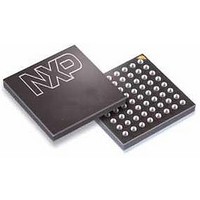
LPC1788FET208,551 NXP Semiconductors, LPC1788FET208,551 Datasheet - Page 47

LPC1788FET208,551
Manufacturer Part Number
LPC1788FET208,551
Description
MCU ARM 512K FLASH 208-TFBGA
Manufacturer
NXP Semiconductors
Series
LPC17xxr
Specifications of LPC1788FET208,551
Core Processor
ARM® Cortex-M3™
Core Size
32-Bit
Speed
100MHz
Connectivity
CAN, EBI/EMI, Ethernet, I²C, Microwire, MMC, SPI, SSI, SSP, UART/USART, USB OTG
Peripherals
Brown-out Detect/Reset, DMA, I²S, LCD, Motor Control PWM, POR, PWM, WDT
Number Of I /o
165
Program Memory Size
512KB (512K x 8)
Program Memory Type
FLASH
Eeprom Size
4K x 8
Ram Size
96K x 8
Voltage - Supply (vcc/vdd)
2.4 V ~ 3.6 V
Data Converters
A/D 8x12b, D/A 1x10b
Oscillator Type
Internal
Operating Temperature
-40°C ~ 85°C
Package / Case
208-TFBGA
Processor Series
LPC178x
Core
ARM Cortex M3
Data Bus Width
32 bit
Data Ram Size
96 KB
Interface Type
SSP, I2S, USB, JTAG, Serial, UART, I2C, SD/MMC
Maximum Clock Frequency
100 MHz
Number Of Programmable I/os
165
Number Of Timers
4
Operating Supply Voltage
2.4 V to 3.6 V
Maximum Operating Temperature
+ 85 C
Mounting Style
SMD/SMT
Operating Temperature Range
- 40 C to + 85 C
Supply Current (max)
100 mA
Lead Free Status / Rohs Status
Lead free / RoHS Compliant
Other names
568-6691
Available stocks
Company
Part Number
Manufacturer
Quantity
Price
Company:
Part Number:
LPC1788FET208,551
Manufacturer:
NXP Semiconductors
Quantity:
10 000
NXP Semiconductors
LPC178X_7X
Objective data sheet
7.12.1 Features
7.11.1 Features
7.12 CRC engine
The Cyclic Redundancy Check (CRC) generator with programmable polynomial settings
supports several CRC standards commonly used. To save system power and bus
bandwidth, the CRC engine supports DMA transfers.
•
•
•
•
•
•
•
•
•
•
•
•
•
•
•
•
•
•
•
•
Eight DMA channels. Each channel can support an unidirectional transfer.
16 DMA request lines.
Single DMA and burst DMA request signals. Each peripheral connected to the DMA
Controller can assert either a burst DMA request or a single DMA request. The DMA
burst size is set by programming the DMA Controller.
Memory-to-memory, memory-to-peripheral, peripheral-to-memory, and
peripheral-to-peripheral transfers are supported.
Scatter or gather DMA is supported through the use of linked lists. This means that
the source and destination areas do not have to occupy contiguous areas of memory.
Hardware DMA channel priority.
AHB slave DMA programming interface. The DMA Controller is programmed by
writing to the DMA control registers over the AHB slave interface.
One AHB bus master for transferring data. The interface transfers data when a DMA
request goes active.
32-bit AHB master bus width.
Incrementing or non-incrementing addressing for source and destination.
Programmable DMA burst size. The DMA burst size can be programmed to more
efficiently transfer data.
Internal four-word FIFO per channel.
Supports 8, 16, and 32-bit wide transactions.
Big-endian and little-endian support. The DMA Controller defaults to little-endian
mode on reset.
An interrupt to the processor can be generated on a DMA completion or when a DMA
error has occurred.
Raw interrupt status. The DMA error and DMA count raw interrupt status can be read
prior to masking.
Supports three common polynomials CRC-CCITT, CRC-16, and CRC-32.
– CRC-CCITT: x
– CRC-16: x
– CRC-32: x
Bit order reverse and 1’s complement programmable setting for input data and CRC
sum.
Programmable seed number setting.
Supports CPU PIO or DMA back-to-back transfer.
All information provided in this document is subject to legal disclaimers.
16
32
+ x
+ x
16
15
26
+ x
Rev. 2 — 27 May 2011
+ x
+ x
12
2
23
+ x
+ 1
+ x
5
+ 1
22
+ x
16
+ x
12
+ x
32-bit ARM Cortex-M3 microcontroller
11
+ x
10
+ x
8
+ x
LPC178x/7x
7
+ x
© NXP B.V. 2011. All rights reserved.
5
+ x
4
+ x
2
47 of 117
+ x + 1


