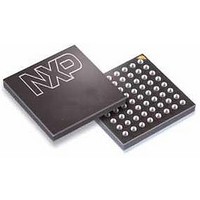
LPC1788FET208,551 NXP Semiconductors, LPC1788FET208,551 Datasheet - Page 62

LPC1788FET208,551
Manufacturer Part Number
LPC1788FET208,551
Description
MCU ARM 512K FLASH 208-TFBGA
Manufacturer
NXP Semiconductors
Series
LPC17xxr
Specifications of LPC1788FET208,551
Core Processor
ARM® Cortex-M3™
Core Size
32-Bit
Speed
100MHz
Connectivity
CAN, EBI/EMI, Ethernet, I²C, Microwire, MMC, SPI, SSI, SSP, UART/USART, USB OTG
Peripherals
Brown-out Detect/Reset, DMA, I²S, LCD, Motor Control PWM, POR, PWM, WDT
Number Of I /o
165
Program Memory Size
512KB (512K x 8)
Program Memory Type
FLASH
Eeprom Size
4K x 8
Ram Size
96K x 8
Voltage - Supply (vcc/vdd)
2.4 V ~ 3.6 V
Data Converters
A/D 8x12b, D/A 1x10b
Oscillator Type
Internal
Operating Temperature
-40°C ~ 85°C
Package / Case
208-TFBGA
Processor Series
LPC178x
Core
ARM Cortex M3
Data Bus Width
32 bit
Data Ram Size
96 KB
Interface Type
SSP, I2S, USB, JTAG, Serial, UART, I2C, SD/MMC
Maximum Clock Frequency
100 MHz
Number Of Programmable I/os
165
Number Of Timers
4
Operating Supply Voltage
2.4 V to 3.6 V
Maximum Operating Temperature
+ 85 C
Mounting Style
SMD/SMT
Operating Temperature Range
- 40 C to + 85 C
Supply Current (max)
100 mA
Lead Free Status / Rohs Status
Lead free / RoHS Compliant
Other names
568-6691
Available stocks
Company
Part Number
Manufacturer
Quantity
Price
Company:
Part Number:
LPC1788FET208,551
Manufacturer:
NXP Semiconductors
Quantity:
10 000
NXP Semiconductors
LPC178X_7X
Objective data sheet
7.33.1.3 RTC oscillator
7.33.1.4 Watchdog oscillator
7.33.2 Main PLL (PLL0) and Alternate PLL (Alt PLL, PLL1)
The RTC oscillator provides a 1 Hz clock to the RTC and a 32 kHz clock output that can
be output on the CLKOUT pin in order to allow trimming the RTC oscillator without
interference from a probe.
The Watchdog Timer has a dedicated oscillator that provides a 500 kHz clock to the
Watchdog Timer that is always running if the Watchdog Timer is enabled. The Watchdog
oscillator clock can be output on the CLKOUT pin in order to allow observe its frequency.
In order to allow Watchdog Timer operation with minimum power consumption, which can
be important in reduced power modes, the Watchdog oscillator frequency is not tightly
controlled. The Watchdog oscillator frequency will vary over temperature and power
supply within a particular part, and may vary by processing across different parts. This
variation should be taken into account when determining Watchdog reload values.
Within a particular part, temperature and power supply variations can produce up to a
17 % frequency variation. Frequency variation between devices under the same
operating conditions can be up to 30 %.
PLL0 (also called the Main PLL) and PLL1 (also called the Alt PLL) are functionally
identical, but have somewhat different input possibilities and output connections. These
possibilities are shown in
or the main oscillator, and can potentially be used to provide the clocks to nearly
everything on the device. The Alternate PLL receives its input only from the main oscillator
and is intended to be used as an alternate source of clocking to the USB. The USB has
timing needs that may not always be filled by the Main PLL.
Both PLLs are disabled and powered off on reset. If the Alternate PLL is left disabled, the
USB clock can be supplied by PLL0 if everything is set up to provide 48 MHz to the USB
clock through that route. The source for each clock must be selected via the CLKSEL
registers, and can be further reduced by clock dividers as needed.
PLL0 accepts an input clock frequency from either the IRC or the main oscillator. If only
the Main PLL is used, then its output frequency must be an integer multiple of all other
clocks needed in the system. PLL1 takes its input only from the main oscillator, requiring
an external crystal in the range of 10 to 25 MHz. In each PLL, the Current Controlled
Oscillator (CCO) operates in the range of 156 MHz to 320 MHz, so there are additional
dividers to bring the output down to the desired frequencies. The minimum output divider
value is 2, insuring that the output of the PLLs have a 50 % duty cycle.
If the USB is used, the possibilities for the CPU clock and other clocks will be limited by
the requirements that the frequency be precise and very low jitter, and that the PLL0
output must be a multiple of 48 MHz. Even multiples of 48 MHz that are within the
operating range of the PLL are 192 MHz and 288 MHz. Also, only the main oscillator in
conjunction with the PLL can meet the precision and jitter specifications for USB. It is due
to these limitations that the Alt PLL is provided.
The alternate PLL accepts an input clock frequency from the main oscillator in the range
of 10 MHz to 25 MHz only. When used as the USB clock, the input frequency is multiplied
up to a multiple of 48 MHz (192 MHz or 288 MHz as described above).
All information provided in this document is subject to legal disclaimers.
Rev. 2 — 27 May 2011
Figure
7. The Main PLL can receive its input from either the IRC
32-bit ARM Cortex-M3 microcontroller
LPC178x/7x
© NXP B.V. 2011. All rights reserved.
62 of 117


