MC88LV926DWR2 Freescale Semiconductor, MC88LV926DWR2 Datasheet
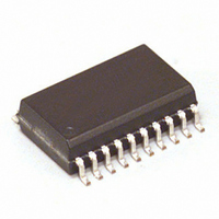
IC DRIVER CLK PLL 66MHZ 20-SOIC

MC88LV926DWR2

Manufacturer Part Number
MC88LV926DWR2
Description
IC DRIVER CLK PLL 66MHZ 20-SOIC
Manufacturer
Freescale Semiconductor
Type
PLL Clock Driverr
Datasheet

Specifications of MC88LV926DWR2

Input
CMOS, TTL
Output
CMOS
Frequency - Max
66MHz
Voltage - Supply
3 V ~ 3.6 V
Operating Temperature
0°C ~ 70°C
Mounting Type
Surface Mount
Package / Case
20-SOIC (7.5mm Width)
Frequency-max
66MHz
Lead Free Status / RoHS Status
Contains lead / RoHS non-compliant
Other names
MC88LV926DWR2TR

Available stocks

Company
Part Number
Manufacturer
Quantity
Price
Company:
Part Number:
MC88LV926DWR2
Quantity:
1 000
MOTOROLA
SEMICONDUCTOR TECHNICAL DATA
Low Skew CMOS PLL 68060
Clock Driver
to lock its low skew outputs’ frequency and phase onto an input reference
clock. It is designed to provide clock distribution for CISC microprocessor
or single processor RISC systems. The RST_IN/RST_OUT(LOCK) pins
provide a processor reset function designed specifically for the
MC68/EC/LC030/040/060 microprocessor family. To support the 68060
processor, the 88LV926 operates from a 3.3V as well as a 5.0V supply.
clock input and distribute it with essentially zero delay to multiple
locations on a board. The PLL also allows the MC88LV926 to multiply a
low frequency input clock and distribute it locally at a higher (2X) system
frequency.
the ‘Q’ output frequency. The 2X_Q output is ideal for 68060 systems which require a 2X processor clock input, and it meets the
tight duty cycle spec of the 50 and 66MHz 68060. The QCLKEN output is designed to drive the CLKEN input of the 68060 when
the bus logic runs at half of the microprocessor clock rate. The QCLKEN output is skewed relative to the 2X_Q output to ensure
that CLKEN setup and hold times of the 68060 are satisfied. A Q/2 frequency is fed back internally, providing a fixed 2X
multiplication from the ‘Q’ outputs to the SYNC input. Since the feedback is done internally (no external feedback pin is provided)
the input/output frequency relationships are fixed. The Q3 output provides an inverted clock output to allow flexibility in the clock
tree design.
88LV926 in a static ‘test mode’. In this mode there is no frequency limitation on the input clock, which is necessary for a low
frequency board test environment.
pin will be pulled actively low until phase–lock is achieved. When phase–lock occurs, the RST_OUT(LOCK) is released and a
pull–up resistor will pull the signal high. To give a processor reset signal, the RST_IN pin is toggled low, and the
RST_OUT(LOCK) pin will stay low for 1024 cycles of the ‘Q’ output frequency after the RST_IN pin is brought back high.
Description of the RST_IN/RST_OUT(LOCK) Functionality
acting as a lock indicator. If the RST_IN pin is held high during system power–up, the RST_OUT pin will be in the low state until
steady state phase/frequency lock to the input reference is achieved. 1024 ‘Q’ output cycles after phase–lock is achieved the
RST_OUT(LOCK) pin will go into a high impedance state, allowing it to be pulled high by an external pull–up resistor (see the
AC/DC specs for the characteristics of the RST_OUT(LOCK) pin). If the RST_IN pin is held low during power–up, the
RST_OUT(LOCK) pin will remain low.
05/01
Motorola, Inc. 2001
2X_Q Output Meets All Requirements of the 50 and 66MHz 68060
Microprocessor PCLK Input Specifications
Low Voltage 3.3V V CC
Three Outputs (Q0–Q2) With Output–Output Skew <500ps
CLKEN Output for Half Speed Bus Applications
The Phase Variation From Part–to–Part Between SYNC and the ‘Q’
Outputs Is Less Than 600ps (Derived From the T PD Specification,
Which Defines the Part–to–Part Skew)
SYNC Input Frequency Range From 5MHZ to 2X_Q F Max /4
All Outputs Have 36mA Drive (Equal High and Low) CMOS Levels
Can Drive Either CMOS or TTL Inputs. All Inputs Are TTL–Level Compatible with V CC = 3.3V
Test Mode Pin (PLL_EN) Provided for Low Frequency Testing
The MC88LV926 Clock Driver utilizes phase–locked loop technology
The PLL allows the high current, low skew outputs to lock onto a single
Three ‘Q’ outputs (Q0–Q2) are provided with less than 500ps skew between their rising edges. A 2X_Q output runs at twice
In normal phase–locked operation the PLL_EN pin is held high. Pulling the PLL_EN pin low disables the VCO and puts the
The RST_OUT(LOCK) pin doubles as a phase–lock indicator. When the RST_IN pin is held high, the open drain RST_OUT
The RST_IN and RST_OUT(LOCK) pins provide a 68030/040/060 processor reset function, with the RST_OUT pin also
1
REV 4
LOW SKEW CMOS PLL
68060 CLOCK DRIVER
MC88LV926
PLASTIC SOIC PACKAGE
20
DW SUFFIX
CASE 751D
1
Order this document
by MC88LV926/D

Related parts for MC88LV926DWR2

MC88LV926DWR2 Summary of contents

Page 1

MOTOROLA SEMICONDUCTOR TECHNICAL DATA Low Skew CMOS PLL 68060 Clock Driver The MC88LV926 Clock Driver utilizes phase–locked loop technology to lock its low skew outputs’ frequency and phase onto an input reference clock designed to provide clock distribution ...

Page 2

MC88LV926 Pinout: 20–Lead Wide SOIC Package (Top View) Description of the RST_IN/RST_OUT(LOCK) Functionality (continued) After the system start–up is complete and the 88LV926 is phase–locked to the SYNC input signal (RST_OUT high), the processor reset functionality can be utilized. When ...

Page 3

MAXIMUM RATINGS* Symbol Supply Voltage Referenced to GND Input Voltage (Referenced to GND) V out DC Output Voltage (Referenced to GND Input Current, Per Pin I out DC ...

Page 4

MC88LV926 LOCK INDICATOR RST_IN RESET_OUT SYNC1 PFD PUMP PLL_EN POWER–ON RESET MR Figure 1. MC88LV926 Logic Block Diagram SYNC INPUT TIMING REQUIREMENTS Symbol t RISE/FALL Rise/Fall Time, SYNC Input SYNC Input From 0.8V to 2.0V t CYCLE ...

Page 5

AC CHARACTERISTICS ( 3.3V Symbol Parameter t RISE/FALL Rise/Fall Time, into 50 Load All Outputs t RISE/FALL Rise/Fall Time into a 50 Load 2X_Q Output t pulse width(a) 1 Output ...

Page 6

MC88LV926 1. Several specifications can only be measured when the MC88LV926 is in phase–locked operation not possible to have the part in phase–lock on ATE (automated test equipment). Statistical characterization techniques were used to guarantee those specifications which ...

Page 7

CRYSTAL OSCILLATOR Figure 4. Logical Representation of the MC88LV926 With Input/Output Frequency Relationships SYNC Input t SKEWall Q0–Q3 Outputs 2X_Q Output QCLKEN t SKEWQCLKEN Figure 5. Output/Input Switching Waveforms and Timing Relationships 1. The MC88LV926 aligns rising edges of ...

Page 8

MC88LV926 The t PD spec includes the full temperature range from and the full V CC range from 3.0V to 3.3V. If the T and given system are less than the ...

Page 9

X–TAL OSCILLATOR SYSTEM RESET Figure 7. Typical MC88LV926/MC68060 System Configuration TIMING SOLUTIONS MC68060 66MHz 2X_Q PCLK SYNC QCLKEN CLKEN 33MHz RST_IN Q3 RST_OUT 9 MC88LV926 ASIC RESET ASIC MEMORY MODULE MOTOROLA ...

Page 10

MC88LV926 10X 0. 20X 0. 18X MOTOROLA OUTLINE DIMENSIONS DW SUFFIX SOIC PACKAGE CASE 751D-06 ISSUE ...

Page 11

TIMING SOLUTIONS NOTES 11 MC88LV926 MOTOROLA ...

Page 12

MC88LV926 Motorola reserves the right to make changes without further notice to any products herein. Motorola makes no warranty, representation or guarantee regarding the suitability of its products for any particular purpose, nor does Motorola assume any liability arising out ...

Related keywords