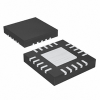
MAX3992UTG+ Maxim Integrated Products, MAX3992UTG+ Datasheet

MAX3992UTG+
Specifications of MAX3992UTG+
Related parts for MAX3992UTG+
MAX3992UTG+ Summary of contents
Page 1
... LOS Indicator ♦ LOL Indicator ♦ Power Dissipation: 356mW leaves RMS PART MAX3992UTG MAX3992UTG+* *Future product—contact factory for availability. +Denotes lead-free package. Applications TOP VIEW *THE EXPOSED PAD MUST BE CONNECTED TO CIRCUIT-BOARD GROUND FOR PROPER THERMAL AND ELECTRICAL PERFORMANCE. with Equalizer ...
Page 2
Clock and Data Recovery with Equalizer ABSOLUTE MAXIMUM RATINGS Supply Voltage, V ..............................................-0.5V to +4.0V CC Input Voltage Levels (SDI+, SDI-, REFCLK+, REFCLK-) ....................................(V CC CML Output Voltage (SDO+, SDO-, SCLKO+, SLCKO-) ......................................(V CC Stresses beyond those listed under ...
Page 3
ELECTRICAL CHARACTERISTICS (continued) (See Table 1 for operating conditions. Typical values at V PARAMETER SYM JITTER SPECIFICATION Jitter Peaking Jitter Transfer Bandwidth Sinusoidal Jitter Tolerance Jitter Generation Serial-Data Output Deterministic Jitter PLL ACQUISITION/LOCK SPECIFICATION Acquisition Time LOL ...
Page 4
Clock and Data Recovery with Equalizer ELECTRICAL CHARACTERISTICS (continued) (See Table 1 for operating conditions. Typical values at V Note 1: Measured with 100mV differential amplitude. P-P Note 2: Guaranteed by design and characterization. Note 3: Measured from the ...
Page 5
AND ACQUISITION TIME ARE DEFINED WITH A VALID REFERENCE CLOCK APPLIED. Figure 1. TX LOL Assert and PLL Acquisition Time DATA INPUT POWER LOS ASSERT TIME LOS LOL Figure 2. LOS Assert/Deassert Time _______________________________________________________________________________________ 10Gbps Clock ...
Page 6
Clock and Data Recovery with Equalizer (V = 3.3V +25°C, unless otherwise noted MAX3992 INPUT (15in FR-4) MAX3992 toc01 500 50 -50 -500 1 0 0.35 0.65 NORMALIZED BIT TIME (UI) POWER-SUPPLY INDUCED OUTPUT JITTER ...
Page 7
T = +25°C, unless otherwise noted COMMON MODE S11 SCC11 0 XFI MASK -5 -10 -15 -20 -25 -30 -35 -40 10M 100M 1G FREQUENCY (Hz) PIN NAME 1, 6, 11, 13 +3.3V ...
Page 8
Clock and Data Recovery with Equalizer PIN NAME Negative Reference Clock Input, Digital. The REFCLK inputs are designed to be AC-coupled to the 22 REFCLK- reference clock source. REFCLK± have a 200Ω differential impedance. See the Detailed Description section ...
Page 9
Loss-of-Lock Monitor The LOL output indicates that the frequency difference between the recovered clock and the reference clock is excessive. LOL may assert due to excessive jitter at the data input, incorrect frequency, or loss of input data. The LOL ...
Page 10
Clock and Data Recovery with Equalizer V CC 50Ω 50Ω SDI+ SDI- Figure 5. CML Input Model VCC 50Ω 50Ω GND Figure 6. CML Output Model 10 ______________________________________________________________________________________ Applications Information The exposed pad, 24-pin QFN incorporates features that provide ...
Page 11
Clock and Data Recovery 0.047µF TOSA SDO+ MAX3975 MAX3992 DRIVER SDO- DS1862* CONTROLLER 2 SDI+ ROSA MAX3991 SDI- 0.047µF ______________________________________________________________________________________ with Equalizer Typical Application Circuit V CC SDI+ SDI- REFCLK+ REFCLK- GND 2 2-WIRE INTERFACE N.C. REFCLK+ REFCLK- SDO+ ...
Page 12
... Maxim cannot assume responsibility for use of any circuitry other than circuitry entirely embodied in a Maxim product. No circuit patent licenses are implied. Maxim reserves the right to change the circuitry and specifications without notice at any time. 12 ____________________Maxim Integrated Products, 120 San Gabriel Drive, Sunnyvale, CA 94086 408-737-7600 © 2006 Maxim Integrated Products (The package drawing(s) in this data sheet may not reflect the most current specifications ...


