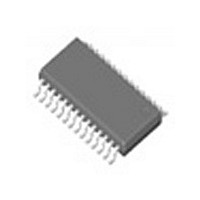
IDTCSPT855PGG IDT, Integrated Device Technology Inc, IDTCSPT855PGG Datasheet - Page 3

IDTCSPT855PGG
Manufacturer Part Number
IDTCSPT855PGG
Description
IC PLL CLK DRIVER 2.5V 28-TSSOP
Manufacturer
IDT, Integrated Device Technology Inc
Type
PLL Clock Driverr
Series
-r
Datasheet
1.IDTCSPT855PG8.pdf
(10 pages)
Specifications of IDTCSPT855PGG
Input
Clock
Output
Clock
Frequency - Max
220MHz
Voltage - Supply
2.3 V ~ 2.7 V
Operating Temperature
0°C ~ 70°C
Mounting Type
Surface Mount
Package / Case
28-TSSOP
Frequency-max
220MHz
Number Of Elements
1
Operating Supply Voltage (typ)
2.5V
Operating Temp Range
0C to 70C
Package Type
TSSOP
Operating Supply Voltage (min)
2.3V
Operating Supply Voltage (max)
2.7V
Operating Temperature Classification
Commercial
Pin Count
28
Lead Free Status / RoHS Status
Lead free / RoHS Compliant
Other names
CSPT855PGG
Available stocks
Company
Part Number
Manufacturer
Quantity
Price
Company:
Part Number:
IDTCSPT855PGG
Manufacturer:
IDT
Quantity:
629
Part Number:
IDTCSPT855PGGI
Manufacturer:
IDT
Quantity:
20 000
FUNCTION TABLE
NOTES:
1. H = HIGH Voltage Level
2. Typically 10MHz.
RECOMMENDED OPERATING CONDITIONS
NOTES:
1. Unused inputs must be held HIGH or LOW to prevent them from floating.
2. DC input signal voltage specifies the allowable DC execution of differential input.
3. Differential input signal voltage specifies the differential voltage | V
4. Differential cross-point voltage is expected to track variations of V
IDTCSPT855
2.5V PLL CLOCK DRIVER
AV
Symbol
L = LOW Voltage Level
Z = High-Impedance OFF-State
X = Don't Care
2.5V (nom)
2.5V (nom)
2.5V (nom)
DD,
V
V
V
V
I
SR
V
I
O(X)
T
OH
OL
AV
GND
GND
I(X)
IH
ID
IL
A
V
X
X
DDQ
DD
Supply Voltage
Input Voltage LOW
Input Voltage HIGH
DC Input Signal Voltage
Differential Input Signal Voltage
Output Differential Cross-Voltage
Input Differential Pair Cross-Voltage
HIGH-Level Output Current
LOW-Level Output Current
Input Slew Rate, see figure 8
Operating Free-Air Temperature
PWRDWN
H
H
H
H
L
L
X
INPUTS
(1)
<20MHz
CLK
(2)
H
H
H
L
L
L
(2)
Parameter
(3)
(4)
(4)
<20MHz
CLK
H
H
H
L
L
L
CLK, CLK, FBIN, FBIN
PRWDWN
CLK, CLK, FBIN, FBIN
PRWDWN
CLK, FBIN
Commercial
Industrial
DDQ
(2)
TR
- V
and is the voltage at which the differential signals must be crossing.
CP
| required for switching, where V
H
H
Y
L
Z
Z
L
Z
3
(1)
COMMERCIAL AND INDUSTRIAL TEMPERATURE RANGES
H
H
Y
L
Z
Z
L
Z
V
V
V
DDQ
DDQ
DDQ
TR
Min.
- 0.3
- 0.3
0.36
2.3
/2 + 0.18
1.7
-40
—
—
—
OUTPUTS
/2 - 0.2
/2 - 0.2
1
0
is the true input level and V
FBOUT
H
H
L
Z
Z
L
Z
V
Typ.
DDQ
—
—
—
—
—
—
—
—
—
—
—
—
—
FBOUT
/2
H
H
L
Z
Z
L
Z
CP
is the complementary input level.
V
V
V
V
V
DDQ
DDQ
DDQ
DDQ
DDQ
Max.
V
- 12
+70
+85
2.7
0.7
/2 - 0.18
—
DDQ
12
/2 + 0.2
/2 + 0.2
Bypassed/OFF
Bypassed/OFF
4
+ 0.3
+ 0.6
OFF
OFF
OFF
PLL
O N
O N
V/ns
Unit
mA
mA
°
V
V
V
V
V
V
V
C


