CY7B991V-7JXC Cypress Semiconductor Corp, CY7B991V-7JXC Datasheet
CY7B991V-7JXC
Specifications of CY7B991V-7JXC
CY7B991V-7JXC
Available stocks


Related parts for CY7B991V-7JXC


CY7B991V-7JXC Summary of contents
Page 1
... Document Number: 38-07141 Rev. *G 3.3-V RoboClock Programmable Skew Clock Buffer Functional Description The CY7B991V 3.3-V RoboClock skew clock buffer (LVPSCB) offers user-selectable control over system clock functions. These multiple output clock drivers provide the system integrator with functions necessary to optimize the timing of high-performance computer systems. ...
Page 2
... Electrical Characteristics................................................. 9 Capacitance .................................................................... 10 Switching Characteristics – 5 Option ........................... 11 Document Number: 38-07141 Rev. *G Switching Characteristics – 7 Option ........................... 12 Ordering Information...................................................... 13 Package Diagram............................................................ 14 Acronyms ........................................................................ 15 Document Conventions ................................................. 15 Document History Page ................................................. 16 Sales, Solutions, and Legal Information ...................... 17 Worldwide Sales and Design Support....................... 17 Products .................................................................... 17 PSoC Solutions ......................................................... 17 CY7B991V Page [+] Feedback ...
Page 3
... Pinouts Figure 1. Pin Configuration – CY7B991V 32-Pin PLCC Package V Table 1. Pin Definition Pin Name Pin Number IO REF 1F0, 1F1 26,27 I 2F0, 2F1 29,30 I 3F0, 3F1 4,5 I 4F0, 4F1 6,7 I TEST 31 I 1Q0, 1Q1 24,23 O 2Q0, 2Q1 20,19 O 3Q0, 3Q1 15,14 O 4Q0, 4Q1 ...
Page 4
... the V and Time Unit Generator (see NOM CO Table 3). The frequency appearing at the REF and FB inputs NOM has reached 2 CY7B991V Table 3 shows the nine possible output [1] Output Functions 1Q0, 1Q1, 3Q0, 3Q1 4Q0, 4Q1 3F0, 4F0 2Q0, 2Q1 –4t Divide by 2 Divide – ...
Page 5
... HH INVERT Test Mode The TEST input is a three-level input. In normal system operation, this pin is connected to ground, allowing the CY7B991V to operate as explained in the “Block Diagram Description” jumper to ground or be tied LOW through a 100-Ω resistor. This enables an external tester to change the state of these pins. ...
Page 6
... CLOCK Figure 2 shows the LVPSCB configured as a zero skew clock buffer. In this mode, the CY7B991V is the basis for a low-skew clock distribution tree. When all of the function select inputs (×F0, ×F1) are left open, the outputs are aligned and drive a terminated transmission line to an independent load. The FB input is tied to any output in this configuration and the operating frequency range is selected with the FS pin. The low skew specification, coupled with the ability to drive terminated transmission lines (with impedances as low as 50 Ω ...
Page 7
... The LVPSCB performs all of the functions described in this section at the same time. It can multiply by two and four or divide by two (and four) at the same time that it shifts its outputs over a wide range or maintains zero skew between selected outputs. CY7B991V REF 10 MHz 4Q0 4Q1 ...
Page 8
... TEST Figure 9 shows the CY7B991V connected in series to construct a zero skew clock distribution tree between boards. Delays of the downstream clock buffers are programmed to compensate for the wire length (that is, select negative skew equal to the wire delay) necessary to connect them to the master clock source, approximating a zero delay clock tree. Cascaded clock buffers accumulate low frequency jitter because of the non-ideal filtering characteristics of the PLL filter ...
Page 9
... CY7B991V is tested one output at a time, output shorted for less than one second, less than 10% duty cycle. Room temperature only. 8. Total output current per output pair is approximated by the following expression that includes device current plus load current: CY7B991V [(4 + 0.11F) + [((835 – ...
Page 10
... RMS [11] Peak CY7B991V [9]] Max Unit 10 pF 3 0.8 V ≤ TTL Input Test Waveform CY7B991V–2 Min Typ Max Unit 15 – 30 MHz 25 – – 80 5.0 – – ns 5.0 – – ns See Table 2 – 0.05 ...
Page 11
... JR Notes 10. Test measurement levels for the CY7B991V are TTL levels (1 1.5 V). Test conditions assume signal transition times less and output loading as shown in the AC Test Loads and Waveforms unless otherwise specified. 11. Guaranteed by statistical correlation. Tested initially and after any design or process changes that may affect these parameters. ...
Page 12
... Cycle-to-cycle output jitter JR Document Number: 38-07141 Rev. *G Description [ LOW [ MID [ HIGH [13, 14] [13, 15] [12, 16] [13, 17] [13, 17] [13, 17] [18] [19] [19] [11] RMS [11] Peak-to-peak CY7B991V CY7B991V–7 Unit Min Typ Max 15 – 30 MHz 25 – – 80 5.0 – – ns 5.0 – – ns See Table 2 – ...
Page 13
... CY7B991V–2JC CY7B991V–2JCT 500 CY7B991V–5JI CY7B991V–5JIT Pb-free 250 CY7B991V–2JXC CY7B991V–2JXCT 500 CY7B991V–5JXC CY7B991V–5JXCT CY7B991V–5JXI CY7B991V–5JXIT 750 CY7B991V–7JXC CY7B991V–7JXCT Ordering Code Definitions X C/I CY 7B991V -2/ - Document Number: 38-07141 Rev. *G Package Type 32-pin PLCC 32-pin PLCC – ...
Page 14
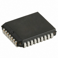
... Package Diagram Figure 11. 32-Pin Plastic Leaded Chip Carrier J65 Document Number: 38-07141 Rev. *G CY7B991V 51-85002 *C Page [+] Feedback ...
Page 15
... Document Number: 38-07141 Rev. *G Document Conventions Table 5. Units of Measure Symbol Unit of Measure °C degree Celsius kΩ kilo ohm µA microamperes µs microsecond mA milliamperes ms millisecond mW milliwatt MHz megahertz ns nanosecond Ω ohm pF pico Farad ps pico second V volts W watts CY7B991V Page [+] Feedback ...
Page 16
... KVM/AESA Format change in Ordering Information Table AESA Change status to final AESA Updated Template, Added Switching Characteristics CY7B991V–2 table. CXQ Changed “100W resistor” to “100Ω resistor” in Test Mode section. Changed “Pb” to “lead” in Ordering Information package type. CXQ Removed inactive part numbers CY7B991V-5JC, CY7B991V-5JCT, CY7B991V-7JC and CY7B991V-7JCT ...
Page 17
... Cypress against all charges. Use may be limited by and subject to the applicable Cypress software license agreement. Document Number: 38-07141 Rev. *G All products and company names mentioned in this document may be the trademarks of their respective holders. cypress.com/go/plc Revised September 29, 2010 CY7B991V PSoC Solutions psoc.cypress.com/solutions PSoC 1 | PSoC 3 ...