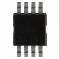
NB6L16DTG ON Semiconductor, NB6L16DTG Datasheet

NB6L16DTG
Specifications of NB6L16DTG
NB6L16DTGOS
Available stocks
Related parts for NB6L16DTG
NB6L16DTG Summary of contents
Page 1
NB6L16 2.5V / 3.3V Multilevel Input to Differential LVPECL/LVNECL Clock or Data Receiver/ Driver/Translator Buffer The NB6L16 is a high precision, low power ECL differential clock or data receiver/driver/translator buffer. The device is functionally equivalent to the EL16, EP16, LVEL16 ...
Page 2
Figure 1. Pinout (Top View) and Logic Diagram Table 1. PIN DESCRIPTION Pin Name I − LVDS, CML, LVPECL, LVNECL, LVTTL, LVCMOS Input 3 D LVDS, CML, LVPECL, LVNECL, LVTTL, LVCMOS Input 4 V − BB ...
Page 3
Table 3. MAXIMUM RATINGS Symbol Parameter V PECL Mode Power Supply CC V NECL Mode Power Supply EE V PECL Mode Input Voltage I NECL Mode Input Voltage I Output Current out V Differential Input Voltage INPP I V Sink/Source ...
Page 4
Table 4. DC CHARACTERISTICS, PECL Symbol Characteristic I Negative Power Supply Current (Note Output HIGH Voltage (Note Output LOW Voltage (Note 6) OL DIFFERENTIAL INPUT DRIVEN SINGLE−ENDED (Figures 10, 12) (Note 8) V Input ...
Page 5
Table 5. DC CHARACTERISTICS, PECL Symbol Characteristic I Negative Power Supply Current (Note 13 Output HIGH Voltage (Note 14 Output LOW Voltage (Note 14) OL DIFFERENTIAL INPUT DRIVEN SINGLE−ENDED (Figures 10, 12) (Note 15) V Input ...
Page 6
Table 6. DC CHARACTERISTICS, NECL Symbol Characteristic I Negative Power Supply Current EE (Note 21) V Output HIGH Voltage (Note 20 Output LOW Voltage (Note 20) OL DIFFERENTIAL INPUT DRIVEN SINGLE−ENDED (Figures 10, 12) (Note 22) V Input ...
Page 7
Table 7. AC CHARACTERISTICS V Symbol Characteristic V Output Voltage Amplitude OUTPP (See Figures 2 & Maximum Operating Data Rate DATA t , Propagation Delay to PLH t Output Differential @ 1 GHz PHL t Duty Cycle Skew ...
Page 8
TIME (62 ps/div) Figure 4. Typical Output Waveform at 23 2.488 Gb/s with PRBS 2 −1 (Total System Pk−Pk Jitter is 16 ps. Device Pk−Pk Jitter Contribution is 3 ps) NOTE: 190 180 170 160 85°C 150 25°C 140 130 ...
Page 9
Figure 10. Differential Input Driven Single−Ended thmax thmin GND Figure 12. V Diagram th Q Driver Device Q Figure 14. Typical Termination for Output ...
Page 10
... ORDERING INFORMATION Device NB6L16D NB6L16DG NB6L16DR2 NB6L16DR2G NB6L16DT NB6L16DTG NB6L16DTR2 NB6L16DTR2G †For information on tape and reel specifications, including part orientation and tape sizes, please refer to our Tape and Reel Packaging Specifications Brochure, BRD8011/D. Resource Reference of Application Notes AN1405/D AN1406/D AN1503/D AN1504/D ...
Page 11
... G C SEATING PLANE −Z− 0.25 (0.010 *For additional information on our Pb−Free strategy and soldering details, please download the ON Semiconductor Soldering and Mounting Techniques Reference Manual, SOLDERRM/D. PACKAGE DIMENSIONS SOIC−8 NB CASE 751−07 ISSUE 0.10 (0.004 SOLDERING FOOTPRINT* 1 ...
Page 12
... Opportunity/Affirmative Action Employer. This literature is subject to all applicable copyright laws and is not for resale in any manner. PUBLICATION ORDERING INFORMATION LITERATURE FULFILLMENT: Literature Distribution Center for ON Semiconductor P.O. Box 5163, Denver, Colorado 80217 USA Phone: 303−675−2175 or 800−344−3860 Toll Free USA/Canada Fax: 303− ...


