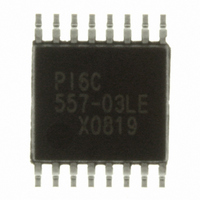
PI6C557-03LE Pericom Semiconductor, PI6C557-03LE Datasheet - Page 6

PI6C557-03LE
Manufacturer Part Number
PI6C557-03LE
Description
IC PCIE CLOCK GENERATIOR 16TSSOP
Manufacturer
Pericom Semiconductor
Type
Clock Generatorr
Datasheet
1.PI6C557-03LE.pdf
(8 pages)
Specifications of PI6C557-03LE
Input
Differential
Output
HSCL
Frequency - Max
125MHz
Voltage - Supply
3 V ~ 3.6 V
Operating Temperature
-40°C ~ 85°C
Mounting Type
Surface Mount
Package / Case
16-TSSOP
Frequency-max
125MHz
Mounting Style
SMD/SMT
Operating Temperature Range
- 40 C to + 85 C
Lead Free Status / RoHS Status
Lead free / RoHS Compliant
Available stocks
Company
Part Number
Manufacturer
Quantity
Price
Company:
Part Number:
PI6C557-03LE
Manufacturer:
PER
Quantity:
480
Part Number:
PI6C557-03LE
Manufacturer:
PERICOM
Quantity:
20 000
Company:
Part Number:
PI6C557-03LEX
Manufacturer:
Hitachi
Quantity:
14
Part Number:
PI6C557-03LEX
Manufacturer:
PERICOM
Quantity:
20 000
Electrical Specifi cations
Maximum Ratings
Recommended Operation Conditions
DC Characteristics (V
Notes:
1. Single edge is monotonic when transitioning through region.
Supply Voltage to Ground Potential ......................................................... 5.5V
All Inputs and Outputs ..................................................... -0.5V to V
Ambient Operating Temperature ................................................ -40 to +80°C
Storage Temperature ................................................................. -65 to +150°C
Junction Temperature ............................................................................150°C
Soldering Temperature ..........................................................................260°C
Parameter
Ambient Operating Temperature
Power Supply Voltage (measured in respect to GND)
Symbol
I
C
R
V
DDOE
L
V
I
C
V
I
OUT
OUT
DD
PIN
DD
IL
IN
IH
IL
07-0274
Parameter
Supply Voltage
Input High Voltage
Input Low Voltage
Input Leakage Current
Operating Supply Current R
Input Capacitance
Output Capacitance
Pin Inductance
Output Resistance
DD
(1)
(1)
= 3.3V ±10%, T
Conditions
S0, S1, OE, CLK, SS0, SS1
S0, S1, OE, CLK, SS0, SS1
0 < Vin < VDD
OE = LOW
Input pin capacitance
Output pin capacitance
CLK Outputs
L
= 50Ω, C
A
L
= -40°C to +85
= 2pF
With input pull-up and
pull-downs
Without input pull-up
and pull-downs
6
DD
+0.5V
o
C)
Note:
Stresses greater than those listed under MAX I MUM RAT-
INGS may cause permanent damage to the de vice. This is
a stress rating only and func tion al op er a tion of the device
at these or any other conditions above those indicated in
the operational sections of this specifi cation is not implied.
Exposure to absolute maximum rating conditions for ex-
tended periods may affect reliability.
Min.
+3.0
-40
GND -0.3
Min.
-20
3.0
2.0
3.0
-5
Typ.
Typ.
3.3
VDD +0.3
PCI Express Clock
Max.
Max.
+3.6
3.60
+85
0.8
20
65
35
PS8824C
5
7
6
5
PI6C557-03
Unit
Unit
mA
mA
μA
nH
kΩ
pF
pF
°C
V
V
V
V
12/14/07


