IDT5V49EE702NDGI8 IDT, Integrated Device Technology Inc, IDT5V49EE702NDGI8 Datasheet - Page 4
IDT5V49EE702NDGI8
Manufacturer Part Number
IDT5V49EE702NDGI8
Description
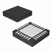
IC PLL CLK GEN 200MHZ 28VQFN
Manufacturer
IDT, Integrated Device Technology Inc
Type
Clock Generator, Multiplexerr
Datasheet
1.IDT5V49EE702NDGI8.pdf
(34 pages)
Specifications of IDT5V49EE702NDGI8
Pll
Yes with Bypass
Input
LVCMOS, LVTTL, Crystal
Output
HCSL, LVCMOS, LVDS, LVPECL, LVTTL
Number Of Circuits
1
Ratio - Input:output
2:7
Differential - Input:output
No/Yes
Frequency - Max
500MHz
Divider/multiplier
Yes/Yes
Voltage - Supply
3.135 V ~ 3.465 V
Operating Temperature
-40°C ~ 85°C
Mounting Type
Surface Mount
Package / Case
28-VQFN Exposed Pad, 28-HVQFN, 28-SQFN, 28-DHVQFN
Frequency-max
500MHz
Lead Free Status / RoHS Status
Lead free / RoHS Compliant
Other names
IDT5V49EE702DLGI8
IDT5V49EE702DLGI8
IDT5V49EE702DLGI8


1.Outputs are user programmable to drive single-ended 3.3-V LVTTL, or differential LVDS, LVPECL or HCSL interface levels
2. When only an individual single-ended clock output is required, tie OUT# and OUT#b together.
IDT® EEPROM PROGRAMMABLE CLOCK GENERATOR
Pin#
IDT5V49EE702
EEPROM PROGRAMMABLE CLOCK GENERATOR
13
14
15
16
17
18
19
20
21
22
23
24
25
26
27
28
Pin Name
CLKSEL
VDDO5
VDDO3
SD/OE
AVDD
SCLK
OUT6
OUT3
OUT0
SDAT
SEL2
SEL1
SEL0
GND
GND
GND
I/O
I/O
O
O
O
I
I
I
I
I
I
Adjustable
Adjustable
Pin Type
LVTTL
LVTTL
LVTTL
LVTTL
LVTTL
LVTTL
LVTTL
LVTTL
Power
Power
Power
Power
Power
Power
1
1
4
Enables/disables the outputs or powers down the chip.
Device power supply. Connect to 1.8 to 3.3V. Sets output
voltage levels for OUT5 and OUT5b.
Connect to Ground.
Bidirectional I
I
Input clock selector. Weak internal pull down resistor.
Device analog power supply. Connect to 3.3V. Use
filtered analog power supply if available.
Connect to Ground.
Configurable clock output 6. Single-ended or differential
when combined with OUT3.
Configurable clock output 3. Single-ended or differential
when combined with OUT6.
Device power supply. Connect to 1.8 to 3.3V. Sets output
voltage levels for OUT3 and OUT6.
Configuration select pin. Weak internal pull down
resistor.
Configuration select pin. Weak internal pull down
resistor.
Configuration select pin. Weak internal pull down
resistor.
The SP bit (0x02) controls the polarity of the signal to be
either active HIGH or LOW. (Default is active HIGH.)
Configurable clock output 0.
Connect to Ground.
2
C clock.
2
C data.
Pin Description
IDT5V49EE702
CLOCK SYNTHESIZER
REV F 022310
Related parts for IDT5V49EE702NDGI8
Image
Part Number
Description
Manufacturer
Datasheet
Request
R

Part Number:
Description:
TRANSLATION DEVICE DPI 80-PQFP
Manufacturer:
IDT, Integrated Device Technology Inc
Datasheet:
Part Number:
Description:
IDT PART
Manufacturer:
IDT, Integrated Device Technology Inc
Datasheet:
Part Number:
Description:
IC LIU T1/E1/J1 OCTAL 256PBGA
Manufacturer:
IDT, Integrated Device Technology Inc
Datasheet:

Part Number:
Description:
IC FREQ TIMING GENERATOR 28TSSOP
Manufacturer:
IDT, Integrated Device Technology Inc
Datasheet:
Part Number:
Description:
IC CLK DVR PLL 1:10 40VFQFPN
Manufacturer:
IDT, Integrated Device Technology Inc
Datasheet:
Part Number:
Description:
IC CLK FANOUT BUFFER 1:18 32LQFP
Manufacturer:
IDT, Integrated Device Technology Inc
Datasheet:
Part Number:
Description:
IC CLK FANOUT BUFFER 1:18 32LQFP
Manufacturer:
IDT, Integrated Device Technology Inc
Datasheet:
Part Number:
Description:
IC CK505 VREG/RES 56TSSOP
Manufacturer:
IDT, Integrated Device Technology Inc
Datasheet:

Part Number:
Description:
IC SDRAM CLK DVR 1:10 48-TSSOP
Manufacturer:
IDT, Integrated Device Technology Inc
Datasheet:

Part Number:
Description:
IC CLK DVR PLL 1:10 48TSSOP
Manufacturer:
IDT, Integrated Device Technology Inc
Datasheet:
Part Number:
Description:
IC FLEXPC CLK PROGR P4 56-TSSOP
Manufacturer:
IDT, Integrated Device Technology Inc
Datasheet:
Part Number:
Description:
IC FLEXPC CLK PROGR P4 56-TSSOP
Manufacturer:
IDT, Integrated Device Technology Inc
Datasheet:
Part Number:
Description:
IC FLEXPC CLK PROGR P4 56-SSOP
Manufacturer:
IDT, Integrated Device Technology Inc
Datasheet:

Part Number:
Description:
IC PLL CLK DRIVER 2.5V 28-TSSOP
Manufacturer:
IDT, Integrated Device Technology Inc
Datasheet:
Part Number:
Description:
IC CLOCK DRIVER 2.5V 24-TSSOP
Manufacturer:
IDT, Integrated Device Technology Inc
Datasheet: