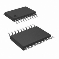
LMX2371TMX National Semiconductor, LMX2371TMX Datasheet - Page 18

LMX2371TMX
Manufacturer Part Number
LMX2371TMX
Description
IC FREQ SYNTH DUAL 20-TSSOP
Manufacturer
National Semiconductor
Series
PLLatinum™r
Type
PLL Frequency Synthesizerr
Datasheet
1.LMX2372TMX.pdf
(24 pages)
Specifications of LMX2371TMX
Pll
Yes with Bypass
Input
CMOS, TTL
Output
CMOS
Number Of Circuits
1
Ratio - Input:output
3:1
Differential - Input:output
Yes/No
Frequency - Max
2GHz, 1.2GHz
Divider/multiplier
Yes/No
Voltage - Supply
2.7 V ~ 5.5 V
Operating Temperature
-40°C ~ 85°C
Mounting Type
Surface Mount
Package / Case
20-TSSOP
Frequency-max
2GHz
Lead Free Status / RoHS Status
Lead free / RoHS Compliant
Other names
*LMX2371TMX
www.national.com
2.0 Programming Description
2.4.4 The FoLD Output Truth Table
X - don’t care condition
Note 10: Open drain lock detect output is provided to indicate when the VCO frequency is in “lock”. When the loop is locked and a lock detect mode is selected,
the pin is HIGH, with narrow pulses LOW. In the Main/Aux lock detect mode a locked condition is indicated when Main and Aux are both locked.
Note 11: The FastLock mode utilizes the FoLD output pin to switch a second loop filter damping resistor to ground during FastLock operation. Activation of FastLock
occurs whenever the Main loop’s ICP
Note 12: Aux and Main PLLs can be reset independently from each other by using the R[18] and R[19] bits. The Aux Counter Reset mode resets Aux PLL’s R and
N counters and brings Aux charge pump output to TRI-STATE condition. The Main Counter Reset mode resets Main PLL’s R and N counters and brings Main charge
pump output to a TRI-STATE condition. The Aux and Main Counter Reset modes reset all counters and bring both charge pump outputs to a TRI-STATE condition.
Upon removal of the Reset bits, the N counter resumes counting in “close” alignment with the R counter. (The maximum error is one prescaler cycle.)
2.5 Serial Data Input Timing
NOTES: Parenthesis data indicates programmable reference divider data.
Data shifted into register on clock rising edge.
Data is shifted in MSB first.
TEST CONDITIONS: The Serial Data Input Timing is tested using a symmetrical waveform around V
amplitudes of 2.2V
R[18]
Main
0
0
1
1
X
X
X
X
0
0
1
1
R[18]
Aux
@
0
1
0
1
0
0
1
1
0
1
0
1
V
CC
= 2.7V and 2.6V
R[19]
Main
0
0
0
0
0
1
0
1
1
1
1
1
o
magnitude bit R[16] is selected HI while the R[18] and R[19] mode bits are set.
@
V
R[19]
CC
Aux
0
0
0
0
1
0
1
0
1
1
1
1
= 5.5V.
Disabled
Aux Lock Detect (Note 10)
Main Lock Detect (Note 10)
Main/Aux Lock Detect (Note 10)
Aux Reference Divider Output
Main Reference Divider Output
Aux Programmable Divider Output
Main Programmable Divider Output
FastLock Output. Open Drain Output (Note 11)
Reset Aux R and N Counters and TRI-STATE Aux Charge Pump (Note 12)
Reset Main R and N Counters and TRI-STATE Main Charge Pump (Note
12)
Reset All Four Counters and TRI-STATE both Charge Pumps (Note 12)
Serial Data Input Timing
(Continued)
18
Fo/LD Output State
CC
/2. The test waveform has an edge rate of 0.6 V/ns with
DS101026-6


